Continue to Site

Welcome to our site!

Electro Tech is an online community (with over 170,000 members) who enjoy talking about and building electronic circuits, projects and gadgets. To participate you need to register. Registration is free. Click here to register now.

  • Welcome to our site! Electro Tech is an online community (with over 170,000 members) who enjoy talking about and building electronic circuits, projects and gadgets. To participate you need to register. Registration is free. Click here to register now.

Touch circuit sound, led. 555 timer

Status
Not open for further replies.
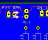
regardless it all worked out. the board looks much better. i made some of those pcb images myself so im probably the reason for that alignment SNAFU.
in all my rambling i neglected to tell you how much this has helped me and i appreciate it. why the file is behaving so badly is a shame but i would spend months writing a program when out of nowhere it starts doing odd things. when that happens i create a new blank document and re-import everything into it. in this case im in unfamiliar territory. i dont know why connections between components are missing or why i cant manually route a track like before but im confident it can be solved.

See post #298.

The problems your experiencing is due to inexperience using the design tool and designing printed circuit boards. Your getting a crash course, so plenty of mistakes are going to made.:smug:

There is another way to look at this, your saving money by not making PCBs that are unusable. :)
 
Last edited:
sorry i did not know. i dont see any way of deleting it. i will try to figure it out.

To remove pour:
click on the pour to hightlight, then right-click and select "clear copper".

To apply pour:
Click on the pour outline to highlight, then right-click and select "pour copper".
 
The problems your experiencing is due to inexperience using the design tool and designing printed circuit boards.
Ill agree with that. as soon as i removed the pours all went well. i remapped the board in no time.
now the only remaing concern i have is the led + / -. They appear to be reversed in the silkscreen. see attached
 

Attachments

  • ledpolarity.jpg
    ledpolarity.jpg
    34.4 KB · Views: 172
Ill agree with that. as soon as i removed the pours all went well. i remapped the board in no time.
now the only remaing concern i have is the led + / -. They appear to be reversed in the silkscreen. see attached

What is the manufacture name and part number for LED?
 
on my demo board i install the leds with the annode facing toward the front of the board. on this silk screen it appears that the led are to be installed with the cathode facing forward.
 
i do not have one. they are 3mm.

on my demo board i install the leds with the annode facing toward the front of the board. on this silk screen it appears that the led are to be installed with the cathode facing forward.

I cannot emphasize this enough:
Know EXACTLY which LED is going to be used or the footprint cannot be relied upon to work.
Find the LED and verify/modify the footprint before using.

This should be done for any part you haven't used before.

The pin-pads on the existing LED footprint look suspiciously large.
 
I understand. This is from a lot of 100 multi colors 3mm leds. So the pin pads look big. Courious, What problems could that cause?

A larger pad can have a "heat sink" effect that will cause more solder and heat required to solder the part. In extreme situations, the extra heat can cause the pad to lift and separate from the pcb. If a high quality LED, a large pad may be ok. But, aside from that, I would verify the distance between the center of the pins.
 
i have edited the file and changed the pad style. the polarity symbols were incorrectly documented. I removed both pours, updated the component, then reapplied both top and bottom pours assigning the GND Net to each. so if this completes the pcb design i thank you.

i have visited the website you recommended (JLC) and selected a 2 layer board. i made some selections and would like your input before i proceed. ive attached a photo. (selection)
 

Attachments

  • ledbefore.jpg
    ledbefore.jpg
    34 KB · Views: 170
  • ledafter.jpg
    ledafter.jpg
    41.4 KB · Views: 170
  • selection.jpg
    selection.jpg
    103.5 KB · Views: 165
i have edited the file and changed the pad style. the polarity symbols were incorrectly documented. I removed both pours, updated the component, then reapplied both top and bottom pours assigning the GND Net to each. so if this completes the pcb design i thank you.

i have visited the website you recommended (JLC) and selected a 2 layer board. i made some selections and would like your input before i proceed. ive attached a photo. (selection)

I recommend to buy a minimum quantity (5) so that you can verify the design.
This is standard practice. There is usually always something that falls through the cracks.;)
Build and test the prototype, and if its good, then buy the remaining quantity.

I know your anxious to buy and build all of them, but I would hate for you buy 20 boards only to find something got overlooked, and they can't be used.


Other than the quantity, the order looks ok.
 
the manufacturing output produced a number of files. i ran autogen and selected all layers for every report. so which ones do i submit? im thinking just the .gbr files
 

Attachments

  • plots.jpg
    plots.jpg
    124.9 KB · Views: 168
the manufacturing output produced a number of files. i ran autogen and selected all layers for every report. so which ones do i submit? im thinking just the .gbr files

Submit all drill data (*.drl) files.

Submit all gerber (*.gbr) files except:
(paste) (this is only for surface mount PCB's)
bottom silkscreen (submit only if you have silkscreen outlines/text on bottom of PCB)
 
I gave them everything. All the gbr and the drill files. I had the order number placed on the bottom so they got that silkscreen file too.
 
Got a request from the manufacturer. Can you help me understand what they want me to do?

Sorry to bother you, but there is an issue that we want to confirm with you before proceeding.
As shown below, the copper layers are the same with the silkscreen layers, and the drill layers seems abnormal.

Could you please fix and replace the file?

much!
m_jZwfAMhH2TMiA5fafohNT0DbByFa-XAPzug6R_8RRFOxAWBiJyeScNu9qVs6qSdOqvf7qQiA4OC28hJpVCSJDDs_C7QPjqOOFhPtMKFiXInCdQnaG-dKerNs6sI_4=s0-d-e1-ft

wSRQ2ttn_teymbpcECGqqJUojNkFfEybCVKh0cHBWHevtMZ6LBfHNRayGA18uHiAY402keEp4JnYD76sD5paH7jxKD6x9r7lJ6XR_cBvu9VmlcVfm-FwjEtHAs9-MCM=s0-d-e1-ft

UBPaxp04IkMyQub8NZcUN2qEYR4rAjha-UeBQs9j5rr4fu7dHZIwj6sDKzjD1l3WhWNj7l95-TQpniKVMkCodfQ3k5AaQS6cl1_k2vEejznd9LnuY3jLwW0EeMQzdC4=s0-d-e1-ft
 
Status
Not open for further replies.

Latest threads

New Articles From Microcontroller Tips

Back
Top