If I were going to manually route this board, here's my approach.
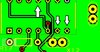
1. Place all parts at locations where placement is critical.
Orient all IC's so notch is in same location.
Place the IC decoupling cap close to the +supply pin of each IC.
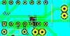
2. Place parts in close "functional block" proximity to each other.
This helps create the shortest track.
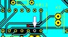
3. When routing tracks, only route tracks between pads and use no more than two connections to pads.
(Do not create a "branch" off of a track).
4. Use 2-sided board (all parts on top).
4.1 Plan to have a "ground" plane on bottom of PCB.
4.2 Route +V tracks and signal tracks on top layer.
4.3 Route signal tracks on bottom layer only when necessary.
4.4 Route +V tracks first and try not to use vias.
4.5 When all tracks have been routed, add a copper pour (ground plane) to bottom layer.
4.6 When all tracks have been routed, add a copper pour (ground plane) to top layer.
The ground planes help keep noise to a minimum.
5. Clean up silkscreen.
Orient text and ref designators so they can all be read with the PCB oriented in one direction
6. Perform design rule check and correct errors.
(No use submitting a PCB for manufacture if it can't be made)")
7. Generate Gerber plots and verify with Gerber file viewer.
Hopefully, if you follow these guidelines you'll have a nice looking PCB designed with a purpose.
1. Place all parts at locations where placement is critical.
Orient all IC's so notch is in same location.
Place the IC decoupling cap close to the +supply pin of each IC.
2. Place parts in close "functional block" proximity to each other.
This helps create the shortest track.
3. When routing tracks, only route tracks between pads and use no more than two connections to pads.
(Do not create a "branch" off of a track).
4. Use 2-sided board (all parts on top).
4.1 Plan to have a "ground" plane on bottom of PCB.
4.2 Route +V tracks and signal tracks on top layer.
4.3 Route signal tracks on bottom layer only when necessary.
4.4 Route +V tracks first and try not to use vias.
4.5 When all tracks have been routed, add a copper pour (ground plane) to bottom layer.
4.6 When all tracks have been routed, add a copper pour (ground plane) to top layer.
The ground planes help keep noise to a minimum.
5. Clean up silkscreen.
Orient text and ref designators so they can all be read with the PCB oriented in one direction
6. Perform design rule check and correct errors.
(No use submitting a PCB for manufacture if it can't be made)
7. Generate Gerber plots and verify with Gerber file viewer.
Hopefully, if you follow these guidelines you'll have a nice looking PCB designed with a purpose.


")