ThomsCircuit
Well-Known Member
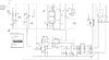
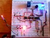
9 months ago I got some help from a few members designing and breadboarding this project. Im new but I'm also determined. With this groups help I have completed other projects too. What this does is open a relay and beep when a sensor is touched. Touch again and it repeats and closes the relay. If will however close the relay on its own after 10-15 miniutes if not manually done. Member eTech helped me with this and i appreciate it. Well I put it together and gave it power. Only the power led and the standby led work. I HAVE studied the breadboard and it does appear correct. I laid it out very neatly so you may be able to see what i may have missed.. I need help now figuring out what is wrong. Thank you in advance. Ive provided the breadboard and schematic in PDF.
")