Continue to Site

Welcome to our site!

Electro Tech is an online community (with over 170,000 members) who enjoy talking about and building electronic circuits, projects and gadgets. To participate you need to register. Registration is free. Click here to register now.

  • Welcome to our site! Electro Tech is an online community (with over 170,000 members) who enjoy talking about and building electronic circuits, projects and gadgets. To participate you need to register. Registration is free. Click here to register now.

Touch circuit sound, led. 555 timer

Status
Not open for further replies.
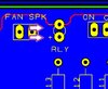
i can see them. some have two and others have more. i assume its because of room and that there are existing tracks going to the pad.

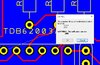
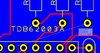
i did get an error when i added the top pour layer. A single pad U3.6 (pin6) did not receive any thermals. the images below show the same area with each layer. is this a problem? the green image is the bottom layer, blue is the top, then one shows both. I can see that the pours did alter my tracks. i can see many tracks in the image that is showing both layers. All very interesting. i hope i have provided you with enough detail to see that i have done a good job here and most importantly that the issue with pin6 is really an issue. it is a DIP socket and not a component.

Pin 6 did not receive a thermal because the pour has no way to connect. It is blocked by tracks. It needs to be corrected.

It would be easier for me to help if you could zip up and post your PCB, schematic, and project file.
And I'll take a look.

If I can I'll fix it and upload. Then we can discuss further
 
i have toyed with this for a while.
i have learned a great deal. i have tried re-routing tracks.
After the bottom pour is done it adds 3 spokes. no room for other spokes from new layer. so i tried removing 2 spokes from the bottom pour but the program adds them back after i apply the second top pour leaving no room for additional spokes. thank you for your assistance.
 

Attachments

  • ClosetTimer.zip
    69 KB · Views: 162
i should tell you the file contains no errors except for the led library component. its in the design of the component. there are 4 errors for each led.
 
i have toyed with this for a while.
i have learned a great deal. i have tried re-routing tracks.
After the bottom pour is done it adds 3 spokes. no room for other spokes from new layer. so i tried removing 2 spokes from the bottom pour but the program adds them back after i apply the second top pour leaving no room for additional spokes. thank you for your assistance.

I'll need a day or two.
 
Hello
I looked over the design and have some comments but too many to list.
I'm uploading a zip file of a modified copy of your design and a zip file of parts.
These files are not meant to replace your design files,. They are only for your review and guidance.

There were a few things a little strange...
1. I changed the layers to appropriate for a double-sided PCB. The top layer was defined as "inner" but should have been "top".
2. I change the units to "thou", precision=3. Easier for me to work with.
3. The resistors and diodes pads were close together. I swapped these parts with suitable footprints I've used in past designs.
4. I also swapped out the IC's and small bypass capacitors.
5. The CD4013 was defined incorrectly.
6. The relay footprint was wired incorrectly.
7. Swapped positions of the 555 and TBD62003.
8. I routed the track for the +5V net.

There is some other stuff but too much to mention.

One thing I noticed was that many of the part pin-pads that should have been on 0.100" centers were not. This made it more difficult to route.
Not your fault. Third party parts sometimes don't work to well. The new parts helped alot.

I left the PCB design unrouted except for the 5V net and the copper pours so you can review.
I've turned off visibility of the nets so as to unobscure the view of the PCB. You can turn this
back on in view->colors-settings and highlights->connections (check-box).
 

Attachments

  • ClosetTimer.zip
    144.4 KB · Views: 178
  • ClosetTimerDonatedParts.zip
    24.3 KB · Views: 167
There is some other stuff but too much to mention.
oh i feel so deflated.
so you know im going to have many q's. my first is the two zip files. i am assuming the first is my original and the other(...donate) are your adjustments. ok surprise! the donated parts. i see. now there are some file extensions here i do not recognize.
before i open these i would like to know what they are
.cmx
.pkg.
.psl
.psx
.ssx
 
Last edited:
oh i feel so deflated.
so you know im going to have many q's. my first is the two zip files. i am assuming the first is my original and the other(...donate) are your adjustments.

the first is the modified version of your original.
The other contains the libraries

don’t feel deflated.
Anyone who designs pcbs has been here before.;)
 

Attachments

  • ledpolarity.jpg
    ledpolarity.jpg
    34.4 KB · Views: 176
unable to map this short ground from the led to the resistor. says the gap is not large enough. im puzzled.
 

Attachments

  • error.jpg
    error.jpg
    67.8 KB · Views: 182
strange.
this short track from R11 to pin 14 throws a warning. says im about to merge this with ground when im just tring to route it. i know what it means and ive accidentally experienced this before but im only routing it. im getting this with other tracks. im also experiencing screen redraw issues. the board will go all white or blue, the tracks dissapear, some tracks are in such a state i cannot locate them. what a mess. its almost impossible to work. ive re-mapped a number of tracks. because of the softwares condition im unable to place vias. its just extremely glitchy. yes i said it. Glitchy.
im not upset. I am a software developer and i know how programs can perform perfectly up untill you place one too many elements on the work area and bam! Your file takes a crap. im continuing to poke away at it but i dont trust the file. so many net/tracks are missing.
 

Attachments

  • neterror1.jpg
    neterror1.jpg
    87.4 KB · Views: 180
  • neterror2.jpg
    neterror2.jpg
    83.9 KB · Views: 170
oh i feel so deflated.
so you know im going to have many q's. my first is the two zip files. i am assuming the first is my original and the other(...donate) are your adjustments. ok surprise! the donated parts. i see. now there are some file extensions here i do not recognize.
before i open these i would like to know what they are
.cmx
.pkg.
.psl
.psx
.ssx

The .??x files were generated by DSPCB. I don't know if they are really needed.
.pkg is the 3D library.
.psl is the PCB footprint library.
 
curious. did i select the wrong component in my schematic?

The schematic symbol is not suitable.
Two logical FF are needed and one set of supply pins so that it correctly maps to the footprint.

is the led labeled incorrectly? the 5v+ rail connects to the negative pad.
OMG. so i will need to re-map ?

Maybe. you need to check the schematic and foot print against the LED datasheet.
 
strange.
this short track from R11 to pin 14 throws a warning. says im about to merge this with ground when im just tring to route it. i know what it means and ive accidentally experienced this before but im only routing it. im getting this with other tracks. im also experiencing screen redraw issues. the board will go all white or blue, the tracks dissapear, some tracks are in such a state i cannot locate them. what a mess. its almost impossible to work. ive re-mapped a number of tracks. because of the softwares condition im unable to place vias. its just extremely glitchy. yes i said it. Glitchy.
im not upset. I am a software developer and i know how programs can perform perfectly up untill you place one too many elements on the work area and bam! Your file takes a crap. im continuing to poke away at it but i dont trust the file. so many net/tracks are missing.

You are not supposed to route tracks with the pour in place.
Remove the pours then route the tracks.
The pour should be applied only after all tracks are routed.

I already explained this.
 
The .??x files were generated by DSPCB. I don't know if they are really needed.
regardless it all worked out. the board looks much better. i made some of those pcb images myself so im probably the reason for that alignment SNAFU.
in all my rambling i neglected to tell you how much this has helped me and i appreciate it. why the file is behaving so badly is a shame but i would spend months writing a program when out of nowhere it starts doing odd things. when that happens i create a new blank document and re-import everything into it. in this case im in unfamiliar territory. i dont know why connections between components are missing or why i cant manually route a track like before but im confident it can be solved.
 
Status
Not open for further replies.

Latest threads

New Articles From Microcontroller Tips

Back
Top