Continue to Site

Welcome to our site!

Electro Tech is an online community (with over 170,000 members) who enjoy talking about and building electronic circuits, projects and gadgets. To participate you need to register. Registration is free. Click here to register now.

  • Welcome to our site! Electro Tech is an online community (with over 170,000 members) who enjoy talking about and building electronic circuits, projects and gadgets. To participate you need to register. Registration is free. Click here to register now.

Touch circuit sound, led. 555 timer

Status
Not open for further replies.
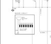
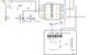
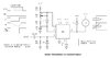
I've laid out the board for both my needs and to reduce wires going all over. Ive also drawn the connections then flipped them so I can make solder connections on the bottom of the board.

That's a good start.

About the pcb design software. I have too many questions. I need to work at this a bit more before I ask for help. I have very little understanding of nets and how I keep them in order. I do think this is key to a good pcb design. Becides I'm learning nothing drawing

A "Net" is a software representation of the connectivity between component connection points. Schematic Capture software (like EasyEDA) uses nets to keep track of this connectivity. One of the outputs of a schematic that has been "captured" is a "netlist" that describes the connectivity contained in the schematic.

You don't have to worry about "keeping them in order". The software does that for you. The software assigns names to each net that follow a pattern recognized by the software. The net names usually look like this: N00032 or N00040 or N00105, etc., but you can rename a net with a more meaningful name if you wish. Sometime you might rename a net to represent a critical part of the wiring, like "VCC" for example, so its easily recognized later in the (PCB) design process ( this allows special handling, like track width for example).

this on paper. Another thing that puzzles me is how do I tell the design software that I have inputs for switches, plugs, jumpers, and terminals? And how does the software know just which adjustable resistor or the type of relay im using? Or that I want to place some components on the other side of the board? Yes. Ive got lots of questions. But I do want to say again. THANK YOU. This was quite the process but it was and still it totally worth all the trouble.

There is a point during the design process where you have to stop and provide the "footprint" information for each physical part. The "footprint" is the physical representation of the PCB "PAD Layout" and physical space required for each part. The schematic symbol is a virtual representation of components (and its pins) contained in a physical part. The physical representation is associated to the schematic representation and follows it through to design completion. Much of this part association is already done in an existing library, but sometimes this needs to be done for non-existent parts.

When your schematic is completed and youve finished part association, you simply "forward" your schematic to the PCB design tool and all parts are placed on a virtual representaion of the PC board. Its your job as the designer to then move/place parts where you need them to be. If a part needs to be placed on the opposite side of the board, you actually place the part on the opposite side of the virtual PC Board. So....in short....what you have drawn on paper, and have shown in the photo, would actually be done on a virtual PC Board.

The design process goes something like this:

Design Requirements->Schematic (Circuit) Capture->Circuit Simulation->Bill Of Materials (physical part list)->PCB design->Mfg Outputs->PCB fabrication->Assembly->Test

There are usually multiple iterations of the process between Schematic capture and PCB design caused by design changes, and sometimes even processes between Schematic capture and Test.

I know all this sounds complicated but it is really not that hard. But it does take discipline.

Hope that helps...
 
Last edited:
I've saved some room on the circuit board and moved the speaker to its own pcb with leads to the other identical boards. Now when any of the boards called for a beep it will come from this one speaker.

My question is now that I've tied all the leads together id like to keep the pulse coming from the circuit calling the buzzer from traveling back through to the other boards. To accomplish this would I add a rectifer diode to each lead?

Note:
The diagram shows just one lead but when complete it will have more leads

Now that I look at this would this even work? The outputs are all high.
 

Attachments

  • 20210208_093235.jpg
    20210208_093235.jpg
    11.6 KB · Views: 152
Now that I look at this would this even work? The outputs are all high.
What am I thinking. This would never work the way it is. I guess I have learned something. So can this be done? It seems it should. Ive got an array of pins all high. If one goes low the buzzer should sound.
 
Hi


The TDA62003 driver outputs switch between ground and high impedence, so you should be able to connect the outputs together without using a diode. However, the buzzer and modules will need to be referenced (connected) to the same +5 volt/ground supply.

BTW-
You can see on the original schematic pins 11+13 are connected together. One output is triggered when the sensor goes from low-to-high, the other output is triggered when the sensor goes from high-to-low.
 
Last edited:
pins 11+13 are connected together.
Oh. I thought they were joined for another reason. To increase the output.
So the out puts (the even pins) are high by default then switched to low to sound the buzzer, light the leds, and trip the relay.
 
Oh. I thought they were joined for another reason. To increase the output.

No. They are joined so the buzzer will "buzz" when either output is low.
In the case of the buzzer, the output is held low only for about 1/2 second.

So the out puts (the even pins) are high by default then switched to low to sound the buzzer, light the leds, and trip the relay.

No. All outputs are either low (ground) or "open" (high impedence).
Each driver input is a logical inverter. So when the input is low, the output is "open". When the input is high, the output is low (ground).
 
Each driver input is a logical inverter. So when the input is low, the output is "open". When the input is high, the output is low (ground).
Right. I understand. The additional parts I needed will be here soon then ill start testing this.
I've got another thing I wanted to do. Its the same as the buzzer but it turns on a 50mmx50mm computer fan only when the relay from any of the 7 circuits is tripped. Basically when the light is on.
I know if I simply tap off the relay that illuminates the light that would work but if I tap all of them and connect to one fan I'd essentially be triggering all the lights when any one relay was tripped. Would this be a condition to insert a diode on each tap so the current won't travel up from one and down the others? In this case grounding all the connections? It would be 12v source.

I see pin 16 on the driver is free. I could use it with a second relay and fan. (one for all) instead of tapping the existing relay
 
Last edited:
Here is a sample drawing of what I would do.

The fan is shown incorrectly. One side of fan would connect to +12, the other thru relay contact to ground (or visa versa, your choice). Also connect a diode across the external relay coil to prevent back EMF. Connect cathode to +5V side of relay and anode to driver side of relay.

There is another option, but it requires a common ground connection between the +12V and +5V power supplies.
Then you could drive the FAN directly from pin 16 without the external relay.
 
but it requires a common ground connection between the +12V and +5V power supplies
Thats just what I have.
A 12v power supply with a few outputs. One would be connected to a buck converter to bring the voltage to 5+
The fans current draw is unknown but its about 70ma. Similar to the relay. And I do thank you very much for your help.

Note: I had edited the image earlier. It should be right (less the diode) now
 
There is another option, but it requires a common ground connection between the +12V and +5V power supplies.
Then you could drive the FAN directly from pin 16 without the external relay.

If you connect as follows, you don't need the external relay.
Connect Pin 1 to Pin 2 at each TDA62003 of each module.
Then connect the FAN like this:

1612829769816.png
 
Thats just what I have.
A 12v power supply with a few outputs. One would be connected to a buck converter to bring the voltage to 5+
The fans current draw is unknown but its about 70ma. Similar to the relay. And I do thank you very much for your help.

Note: I had edited the image earlier. It should be right (less the diode) now

If I had know known, we could have designed the whole circuit to run on 12vdc.
Actually, it wouldn't take much to modify the existing circuit. We'd just have to change a few resistor and cap values. The IC's would remain the same. The Relay and Buzzer would need to change to 12Vdc
 
Yes. I have 12v relays.
Ive been researching a way to keep the fan running after pin 16 goes back to high for 30-60 seconds. The 555 traditionally is triggered low and outputs high so that was my first hurdle. I found an example that triggers on high through pin 6 but still outputs high. I thought I'd connect pin16 to the fan and pin6 of this circuit. When pin16 went back from low to high the timer would trigger but its output on pin3 is high so I did not know how to overcome that. I really was hoping that I could figure this one out myself. I do however understand some of what I'm reading more that I did last year so I'm pleased with that.
 

Attachments

  • Edge-Triggered-555-Monostable-Schematic-1.jpg
    Edge-Triggered-555-Monostable-Schematic-1.jpg
    46.7 KB · Views: 152
Yes. I have 12v relays.
Ive been researching a way to keep the fan running after pin 16 goes back to high for 30-60 seconds. The 555 traditionally is triggered low and outputs high so that was my first hurdle. I found an example that triggers on high through pin 6 but still outputs high. I thought I'd connect pin16 to the fan and pin6 of this circuit. When pin16 went back from low to high the timer would trigger but its output on pin3 is high so I did not know how to overcome that. I really was hoping that I could figure this one out myself. I do however understand some of what I'm reading more that I did last year so I'm pleased with that.

HI

I'm a little confused with what you want the fan to do.

You want the FAN to turn on when any one of 7 relays energize
You want the FAN to stay on untill all 7 relays de-energize.
Then you want the FAN to stay on for 30-60 seconds after all 7 relays de-energize.
So...you want a 30-60 second "delay off" for the fan. Correct?
 
Hi.
Currently the fan is controlled by pin 16. Anytime the fan is turned off via pin 16 I'd like it to turn back on (or stay on) for an additional 30 seconds.
 
Status
Not open for further replies.

Latest threads

New Articles From Microcontroller Tips

Back
Top