Electro Tech is an online community (with over 170,000 members) who enjoy talking about and building electronic circuits, projects and gadgets. To participate you need to register. Registration is free. Click here to register now.
Welcome to our site! Electro Tech is an online community (with over 170,000 members) who enjoy talking about and building electronic circuits, projects and gadgets. To participate you need to register. Registration is free. Click here to register now.
Your circuit seems to be more complicated than it needs to be.
You should have included a brief description of how your circuit works (or how you think it works).
You need to help us if you want us to help you.
The 74283 is an adder but it has the A & B inputs paralled and therefore doubles the input value. I don't understand why.
All you need to determine whether S_AMP is >3 by determining if is D2 = 1
And you don't need the 74175 as it is not necessary to store the switch settings.
I can't work out how your counter works.
You OR Qa, Qb, Qc & Qd but I can't see why.
I would reset the counter when CONFIRM is active and let it count up when CONFIRM is inactive.
Design gating to determine when the S_AMP = 4 and if so, flash the red LED 12 times then change to green. If S_AMP = 5, flash the Red LED 15 times then green once then stop.
If S_AMP < 3, flash green LED 16 times.
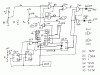
The 1k pull down resistors at the switches (ie. both the push button and the digit switch) should be connected as pull up, not pull down. Pull down is OK with CMOS but not with TTL. The switches should switch gnd, not +5 Volt. You will have to account for the inversion, but that won't be difficult.
Also, TTL is much better at sinking current than sourcing it. So you should connect +5Volt to the LED anodes and the resistors to active low signals.
This project is about a dip switch which control the scale of 0 - 5.
After pressing the pushbutton switch, the timing of the led will light up depending
on the scale.If the scaled is 0 to 3, the green led flashes for 16 times.
If the scale is 3 to 5, the red led flahes for 3 x scale times and after which green
led is flashed for the next (16-(3xscale)) seconds.
Can you advise in my layout in red, as to which part i need to amend? REally appreciate if you could advise further. Thanks.
This is the fourth thread you have running on the same topic.
I have replied a number of times to your questions. [ on your multiple threads] regarding the diagram,
but. you dont seem to change your original drawing.
As I and Len have previously pointed out, the circuit is over complex and will not work as you expect.
Why did the tutor start you off with a 74175 device???
Did you connect the CLEAR and ENBLE pins you asked about??
I would recommend. again, that you re-specify and re-post the project.
What exactly does the project assignment ask you to do?
I need help on the IC 74283 layout.
In order to multiply by 2, you need to left shift 1 bit
For example:
0001 is 1
0010 is 2
0100 is 4
1000 is 8
By left shifting, you multiply by 2. Then by adding to the actual number again, the end result is multiplying by 3.
Therefore the input of the adder A1, A2, A3 should not be connected to B1, B2, B3. It should be shifted. And the unconnected input for the adder should be grounded and need to shift the bit for one the input. Is that correct in my amendment layout on the 74283?
Is my counter counting down? And does my B output and input to And gate is wrong? Please advise. Thanks.
If the counter is configured to count down the red LED will be on for that number of counts.
BUT, your circuit does not meet your tutor's requirements.
1. The circuit must flash the red LED if S_AMP >3.
Your circuit will do it for all S_AMP values. eg. if S_AMP = 2, the red LED will be on for 6 counts.
And the red LED won't flash. It will be on continuously for the number of counts loaded into the counter.
2. The circuit must flash the green LED 16 - 3*S_AMP if S_AMP > 3 and 16 times if S_AMP <4.
The green LED won't flash either.
As I said previously, you don't need to multiply S_AMP by 3. It can be done by gating:-
If S_AMP = 4, flash the red LED 12 times and the green LED 4 times.
If S_AMP = 5, flash the red LED 15 times and the green LED once.
The counter counts down if the correct potential is connected to the D/U input. See the data sheet of the 74191.
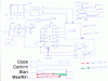
Here is how I would do it. I've included the gating from my previous post. See that post for the explanation. This circuit complies with your tutor's requirements.
Thanks so much for your reply. I have just brought the ic yesterday and will try to do the wiring of urs and try out 1st. Btw, from my circuit layout, beside the adder problem, what other problem is out there?
I got some taiwan brand of ic chip. Can i said for most of the IC chips of 7400, their connection points are the same despite different manufacturer? Please advise. Thanks.
Thanks so much for your reply. I have just brought the ic yesterday and will try to do the wiring of urs and try out 1st. Btw, from my circuit layout, beside the adder problem, what other problem is out there?
I have pointed out the flaws in your circuit in previous posts.
Basically, it does not meet your tutor's requirements.
You need to set the counter to zero, count up and flash the red LED 12 times if S_AMP = 4 and 15 times if S_AMP = 5, and then flash the green LED for 4 times or once respectively.
I got some taiwan brand of ic chip. Can i said for most of the IC chips of 7400, their connection points are the same despite different manufacturer? Please advise. Thanks.
You need to break the question down into the basic logic - as I did in earlier posts.
Then design a circuit to perform that logic.
1. design the gating to provide an output if S_AMP=4 and another output if S_AMP = 5. I used Kanaugh maps.
2. reset the counter when the button is pressed. Since the counter you chose does not have a reset input, I used the load input and set the data inputs to 0.
3. reset the FF at the next clock edge and use its output to open the LED gates.
4. include gating so that the red LED is on for counts 0 ~ 11 if S_AMP=4
5. include gating so that the red LED is on for counts 0 ~ 15 if S_AMP=5
5. do as you did so that the green LED is on once the red one has finished flashing.
6. if S_AMP is <4, don't turn the red LED on so only the green one flashes for the full 16 counts.
7. when Max/Min goes high, set the FF at the next clock edge so the LED gate is closed to prevent further flashing.
8. also gate the clock signal into the LED gating so the LEDs flash at the clock rate.
I initially reset the FF (you initially set the FF) since both K and Load are active low. This allowed me to minimise the number of ICs required.
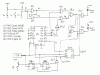
I got a few questions before i start wiring your layout to test out.
Q(1) Does dip switch need 1kohm resistor ?
Do i need 3 1kohm resistor or 2 1kohm resistor?
Q(2) What does max/min 15 refers to?
Q(3) Why does input of U3a and U3b needs to connect to clk?
Q(4) Why 2 input of U3C need to connect to 5v?
Q(5) For Qb bar of U6b, do we need to conenct to gn?
Q(6) For dip switch, why does it need to conenct resistor to 5v?
Q(7) For IC 74191, why does A,B,C,D & En need to conenct to gnd?
These unconected QA & QB, do we need to conenct to any point?
I got a few questions before i start wiring your layout to test out.
Q(1) Does dip switch need 1kohm resistor ?
Do i need 3 1kohm resistor or 2 1kohm resistor?
Q(2) What does max/min 15 refers to?
Q(3) Why does input of U3a and U3b needs to connect to clk?
Q(4) Why 2 input of U3C need to connect to 5v?
Q(5) For Qb bar of U6b, do we need to conenct to gn?
Q(6) For dip switch, why does it need to conenct resistor to 5v?
Q(7) For IC 74191, why does A,B,C,D & En need to conenct to gnd?
Q(8)These unconected QA & QB, do we need to conenct to any point?
A(1) TTL does not need pull up resistors since Open = High. But CMOS does.
So you can insert resistors if you wish. You only need 2 since D1 does not do anything.
A(2) Look at the data sheet for the 74191. Max/Min is high at 15 if the counter is counting up or high at 0 if counting down.
A(3) Because your tutor asked that the LEDs flash. This makes them flash at the clock rate.
A(4) Because it is used as an inverter. Again, you can leave them open if you wish since it is a TTL IC.
A(5) No. Qb bar of U6b is an output and MUST be left open.
A(6) I answered this in A(1)
A(7) If you look at the data sheet, you will see that En is Active Low. So if you want the counter to count, this pin must be connected to gnd.
The A, B, C & D inputs must be connected to gnd so that 0000 will be loaded when the Load pin is set low. This is necessary since the IC does not have a reset pin.
A(8) No. Unused outputs MUST be left open.
A(9) Read the data sheet. This is the up/down control. Low = Up.
Don't forget to connect 100 nF bypass capacitors across the Vcc and gnd pins of the ICs. You may experience strange results if there is insufficient bypassing.
Attached is an alternative gating arrangement that yopu may wish to consider. I've also attached my gating paper for your info.
This site uses cookies to help personalise content, tailor your experience and to keep you logged in if you register.
By continuing to use this site, you are consenting to our use of cookies.