My son is graduating next year with a EE degree.
He can't get his design project to work
He is using a Ti chip (LMG5200MOF -TRANS) but I suspect there is something wrong
he is also using
the problem that he is having is that he is expecting an output of 12V he is actually getting -122.8mV
more info:
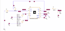
Class D Circuit
48V into Vin
5V into Vcc
Pulse width Modulation (PWM) into the HI and LI
LC circuit from SW output (12V) and (8A)
PWM Frequency is 2048kHz
Need decoupling capacitors in Vin & Vcc
thanks everyone in advance for your help!!
G'
He can't get his design project to work
He is using a Ti chip (LMG5200MOF -TRANS) but I suspect there is something wrong
he is also using
the problem that he is having is that he is expecting an output of 12V he is actually getting -122.8mV
more info:
Class D Circuit
48V into Vin
5V into Vcc
Pulse width Modulation (PWM) into the HI and LI
LC circuit from SW output (12V) and (8A)
PWM Frequency is 2048kHz
Need decoupling capacitors in Vin & Vcc
thanks everyone in advance for your help!!
G'

")
