Continue to Site

Welcome to our site!

Electro Tech is an online community (with over 170,000 members) who enjoy talking about and building electronic circuits, projects and gadgets. To participate you need to register. Registration is free. Click here to register now.

  • Welcome to our site! Electro Tech is an online community (with over 170,000 members) who enjoy talking about and building electronic circuits, projects and gadgets. To participate you need to register. Registration is free. Click here to register now.

Touch circuit sound, led. 555 timer

Status
Not open for further replies.
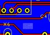
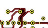
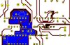
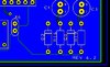
i decided to hide all layers and look at each one at a time. after i did i found an un-routed net. WOW. i also went ahead and edited the led image so the graphic circle no longer overlapped the pads. i don't think those things really had anything to do with what they are referring to.

I also understand that they are using the digital files i provided and not my images so perhaps the options i selected when i generated the report files caused this but im unsure and do appreciate the help. I do hope it is something simple. Regardless, it is a mixed blessing that there was an issue because i would have never caught the un-routed net.

The whole experience brings me back to my developing days. There was a lot of leway with the tools i had but If i had a comma out of place or an extra space the entire page would fail.
 

Attachments

  • un-routed net.jpg
    un-routed net.jpg
    74.7 KB · Views: 178
Got a request from the manufacturer. Can you help me understand what they want me to do?

Sorry to bother you, but there is an issue that we want to confirm with you before proceeding.
As shown below, the copper layers are the same with the silkscreen layers, and the drill layers seems abnormal.

Could you please fix and replace the file?

much!
m_jZwfAMhH2TMiA5fafohNT0DbByFa-XAPzug6R_8RRFOxAWBiJyeScNu9qVs6qSdOqvf7qQiA4OC28hJpVCSJDDs_C7QPjqOOFhPtMKFiXInCdQnaG-dKerNs6sI_4=s0-d-e1-ft

wSRQ2ttn_teymbpcECGqqJUojNkFfEybCVKh0cHBWHevtMZ6LBfHNRayGA18uHiAY402keEp4JnYD76sD5paH7jxKD6x9r7lJ6XR_cBvu9VmlcVfm-FwjEtHAs9-MCM=s0-d-e1-ft

UBPaxp04IkMyQub8NZcUN2qEYR4rAjha-UeBQs9j5rr4fu7dHZIwj6sDKzjD1l3WhWNj7l95-TQpniKVMkCodfQ3k5AaQS6cl1_k2vEejznd9LnuY3jLwW0EeMQzdC4=s0-d-e1-ft

post the zip file you sent to jlcpcb.
 
Last edited:
Submit all drill data (*.drl) files.

Submit all gerber (*.gbr) files except:
(paste) (this is only for surface mount PCB's)
bottom silkscreen (submit only if you have silkscreen outlines/text on bottom of PCB)
I looked up what i could find on producing (generating) the Gerber plots. I had selected all layers for each plot whereas online documentation said to leave as is. The reason i did that was the program through a message when i pressed RUN under the default settings. "No board layer has been selected for any plot"

This time i re-ran the Auto-Gen but I added a GERBER plot and titled it Board Outline. I then just selected (assigned) the board outline layer to my custom plot. Im posting that set of files here.
NOTE: i have not submitted this to the manufacture. I will if you approve.
IVE SINCE RE-RAN THE REPORT ONCE MORE. POST 327
 

Attachments

  • ClosetTimer-REV6-1.zip
    39.4 KB · Views: 161
Last edited:
Throughout the project i would run the design rules check. I selected everything. I would only get a message about the leds silkscreen overlapping the pad. ive since corrected that. I just re-ran it again but i noticed i missed a set of checks. "NETS" how dumb. if i had seen that and had it selected it would have surly warned me about the missing route between R20 & R22. Needless to say ive got these 4 new errors or really existing errors.
if you could help me understand what i should do (if needed) about them in this report.

Results
=======

Gap in Net "GND" between (14619.000,23117.130) and (15156.000,23742.130)
GND.
Gap in Net "GND" between (14619.000,23117.130) and (14469.000,23792.130)
GND.
Gap in Net "GND" between (15974.449,23300.000) and (15719.000,23367.130)
GND.
Dangling Track from (14215.000,23500.000) to (14250.000,23500.000) on layer Bottom Copper

Number of errors found : 4
 

Attachments

  • ReportError.jpg
    ReportError.jpg
    62.9 KB · Views: 175
Last edited:
Gap in Net
Dangling Track
I found them. the net gaps were resolved when i re-poured and removed islands and the dangling track was a tiny route under a pad that i must have not deleted when i was re-routing a track. i deleted that. reran the report and all is good.
 
NEW PLOT FILES

This group of files "Rev6-1-a.zip" are organized ok. However:
1. The top copper has tracks that need correction. review attached.
2. The bottom copper has tracks that need correction. review attached.
3. The bottom silkscreen has random characters on it. Review, then keep or remove.
4. The top/bottom paste is not needed (only for surface mount).

Comments:

4. When you route tracks:
4.1 Try to route the track point to point using 90 degree angles.
4.2 Use no more than 2 track connections per pad.
4.3 After the route is complete, add "45 degree miters" at each "corner".

Now...I'm not suggesting to go back and re-route all the tracks. Use this info for future projects.

5. I don't see any mounting holes (or perhaps I missed them)? How do you plan to attach the PCB to a mounting surface?

Top copper gbr.PNG
Bottom copper gbr.PNG
 
Last edited:
Yes...Rev6.zip set of files is no good.
Apparently, some layers got merged into the same gerber file.

A word on terminology:
The gerber files are not "reports". They are "gerber" data files (gerber files for short).
The drill files are "excellon" data files. They are called "Drill files" for short.
In DSPCB, these files are collectively called "manufacturing plots".

Just thought I'd mention this to keep from getting confused...
 
1. The top copper has tracks that need correction. review attached.
2. The bottom copper has tracks that need correction. review attached.
3. The bottom silkscreen has random characters on it. Review, then keep or remove.
4. The top/bottom paste is not needed (only for surface mount).
I can absolutely do #4
#3 is where the order number goes. (JLCJLCJLCJLC) thats how i was instructed to format the location. it will be replaced with whatever they are going to place there.
#1 & #2 i just do not understand. And i say that with a huge sigh. We have exchanged over 800 posts in the past few months and if there is one thing you have figured out about me is sometimes i need the stupid slapped out of me. This is one of those times. With that being said the software and or my old PC drives me insane with the screen re-draws. Ive posted some examples. Now sometimes it works great. Those are the times where my tracks look awesome. When my tracks look like crap is most likely when the program blindfolds me with white screens, half renders, and other weird stuff. Thoes times i end up setteling for what i can accomplish . Ill attempt to edit the track and add 45 degree leads but the software (and lack of experience) arm wrestles me until I concede. Now this will not stop me from trying to fix the issues but I dont know what it is your wanting me to do. Im going to add 45 degree everywhere i can and separate tracks that may appear too close to another.
 

Attachments

  • Grrr01.jpg
    Grrr01.jpg
    69.1 KB · Views: 170
  • Grrr02.jpg
    Grrr02.jpg
    93.7 KB · Views: 171
I can absolutely do #4
#3 is where the order number goes. (JLCJLCJLCJLC) thats how i was instructed to format the location. it will be replaced with whatever they are going to place there.

OK

#1 & #2 i just do not understand. And i say that with a huge sigh. We have exchanged over 800 posts in the past few months and if there is one thing you have figured out about me is sometimes i need the stupid slapped out of me. This is one of those times. With that being said the software and or my old PC drives me insane with the screen re-draws. Ive posted some examples. Now sometimes it works great. Those are the times where my tracks look awesome. When my tracks look like crap is most likely when the program blindfolds me with white screens, half renders, and other weird stuff. Thoes times i end up setteling for what i can accomplish . Ill attempt to edit the track and add 45 degree leads but the software (and lack of experience) arm wrestles me until I concede. Now this will not stop me from trying to fix the issues but I dont know what it is your wanting me to do. Im going to add 45 degree everywhere i can and separate tracks that may appear too close to another.

I cant do anything about how your computer behaives....but I feel your pain. :cool:

I already stated:
"Now...I'm not suggesting to go back and re-route all the tracks. Use this info for future projects. "

What I've shown you is where the board design could use improvement. You can ignore if you want.
The next action is up to you.

maybe this will help:

1614534341689.png
 
i did what i could to make it better. I received 2 net dangle errors that were difficult to clear but they are gone now.
Oh the mounting holes. The boards will be slid into a pair of miter slots. like the kind you see on all thoes movies where actors are seen ripping out p.c boards to save the planet from self destruction. here are my final data and drill files.
 

Attachments

  • 45 degree changes.jpg
    45 degree changes.jpg
    79.9 KB · Views: 168
  • ClosetTimer-REV6-1-b.zip
    41.8 KB · Views: 160
What I've shown you is where the board design could use improvement. You can ignore if you want.
The next action is up to you.

maybe this will help:
IMAGE NOT SHOWN
thank you. If you have looked at my interpretation prior to your upload of the images showing what good and poor tracks look like youll see that i have not done very well.

On the bright side I have learned to control the route tool pretty well. I had read somewhere to approach the pads on a 45 degree angle so the copper pours can have room to add their thermal reliefs.

I did not know how to remove a net and reconnect elsewhere to avoid having 3 nets on one pad so i had to leave them as is.

More good news.
The manufacture has approved my latest data files so im now in production.

I decided (after the fact) to return to the PCB and have another go at relocating nets. I was successful. I was able to relocate 2. A third had no other possible path. Thank you again for your help.
 
"Now...I'm not suggesting to go back and re-route all the tracks. Use this info for future projects. "
My PCB boards came in. They look real nice.
Ill be soldering one up tomorrow.
I have become pretty comfortable with the program. I plotted the fan delay off circuit you designed and made this PCB. I had no problems relocating tracks that were trippled up on pads and much better at miters. Ive altered the variable resistor library file to suit the ones I have. Snapping components to half grid makes things easier too. Seeing the PCB boards has spoiled me some so I may send this out for production.
Attached net routing. The second one is improved.
 

Attachments

  • FanTimer.jpg
    FanTimer.jpg
    151.8 KB · Views: 172
  • FanTimer2.jpg
    FanTimer2.jpg
    149.2 KB · Views: 170
Last edited:
Status
Not open for further replies.

Latest threads

New Articles From Microcontroller Tips

Back
Top