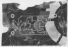
Don't you feel the drill holes of most components are larger. perhaps, for future boards, you may reduce the drill diameter so that each pad can have more copper skin, and the central drill marking can be as small , only to guide the drill bit centering.
That's a good idea, that way, you don't have to use a centre punch before drilling.
as well as component pads.
they look big??
The smallest holes are 1mm - it's my smallest drill bit.
The smallest pads are 2mm wide.
I should have put a ruler in the picture, the board is approximately 35×78mm and is not perfectly square as I can't saw perfectly straight with a hacksaw.
mag paper looks like a good alternative but still wonder about jamming the printer,
That'll only happen if you use really thin paper. I've never had a problem with jamming because the paper I use isn't much thinner than normal copier paper.
how small of a trace is possible etc.
The traces on the boards above are all 0.5mm.
I've never needed to go thinner than 0.5mm but I know 0.25mm (about 0.01 inches) must be possible as I use it for the silk screen.
Yes I can do a silk screen using toner transfer with magazine paper, it's easy to do. Once I've etched and drilled the board, I apply the silk screen layer, using the normal toner transfer with magazine paper, then I cover it with a thin layer of conformal coating to seal it in.
Going to try a 2x board using the transfer sheet folded in half process.
I haven't done a double sided PCB yet. If I do it that's the way I'd do it. Of course you'll need to take the thickness of the board and bend radius of the paper into account.
that's why I etch one side then do a transfer for second side.
How do you etch just one side of the board?
Do you mask off the other side? If so how?
Nice looking board. However when I started out making DIY PCB, I remember not removing the toner first and ended up with with melted toner on the drill bit and messed up pad(s).
I've never had that problem.
Maybe it's because I've made holes in the pads?
Why is the mess a problem?
Can't you just clean the drill bits and the PCB?
I've never tried it but I imagine that it'll be hard to remove.
I would rather be rubbing / scrubbing!
What scrubbing?
I don't need to do any scrubbing, the paper peels fairly cleanly off. There might be the odd bits and pieces that don't come off but I don't need to scrub. I was very lucking with the above board, the paper came completely off and didn't need soaking very long before it peeled.
")