Continue to Site

Welcome to our site!

Electro Tech is an online community (with over 170,000 members) who enjoy talking about and building electronic circuits, projects and gadgets. To participate you need to register. Registration is free. Click here to register now.

  • Welcome to our site! Electro Tech is an online community (with over 170,000 members) who enjoy talking about and building electronic circuits, projects and gadgets. To participate you need to register. Registration is free. Click here to register now.

Moat in PCB

Status
Not open for further replies.

electricity86

New Member
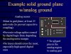
Could someone explain to me please how exactly does one place a moat in a PCB?

It prevents capacitive coupling only between analoag traces and digital traces right?

(can you neglect capacitive coupling between analog traces due to low frequency which means capacitors behave as cutoff?)

Thanks.

a-jpg.27061
 

Attachments

  • a.JPG
    a.JPG
    58.3 KB · Views: 3,030
I'm not good with the theory, but that looks like just a break in the ground plane. If you are using Eagle, just route a large 'wire' the correct width, on the restrict or keepout layer to prevent the ground polygon from filling in that area.
 
The purpose of the moat is to minimize the high speed digital signals on the digital ground plane from corrupting the analog ground plane. It's not related to direct capacitive coupling between analog and digital traces, only indirectly through the ground planes.

One way is to make two separate ground planes and then tie them together with a copper bridge. Another is to do a copper cut or keep-out on a single copper plane.

The technique you use somewhat depends upon the particular capabilities of the PCB software you are using.
 
The meaning in their picture of the phrase "at least 25 mils wide (to prevent capacitive coupling)" means that you have to make the gap at least that wide so that noise currents on one edge of the slot do not couple capacitively to the other edge of the slot. If you make the slot too narrow, high frequency current will "jump" the slot via capacitive coupling and the slot will become useless.
 
Last edited:
If you are using Eagle this is how to make moat:
 

Attachments

  • MOAT.gif
    MOAT.gif
    17.5 KB · Views: 865
That doesn't seem like the same thing that's referenced in the original image. That 'moat' you've exampled is just one big restrict block underneath a chip. The 'moat' in the original image shows a restrict that surrounds that analog sensor area which would decouple the entire secondary ground plane. It doesn't remove the ground plane, it just isolates it.
 
That doesn't seem like the same thing that's referenced in the original image. That 'moat' you've exampled is just one big restrict block underneath a chip. The 'moat' in the original image shows a restrict that surrounds that analog sensor area which would decouple the entire secondary ground plane. It doesn't remove the ground plane, it just isolates it.

From my understanding a moat divides areas like a canal of water as used around fortresses in Europe (with geese as watchdogs).

So the shape of a moat will change with the purpose. From the picture posted here it looked like the area underneath the IC is black and the rest of the PCB looks dark grey.

If in this case the moats are the two thick white lines this can be done the same way.

Boncuk
 
The red line indicates the black chip in the original diagram is the analog sensor.

The second red line indicates the white lines are the 'moat', which surrounds the analog circuit area, partially dividing the ground plane.
 
Status
Not open for further replies.

Latest threads

New Articles From Microcontroller Tips

Back
Top