Continue to Site

Welcome to our site!

Electro Tech is an online community (with over 170,000 members) who enjoy talking about and building electronic circuits, projects and gadgets. To participate you need to register. Registration is free. Click here to register now.

  • Welcome to our site! Electro Tech is an online community (with over 170,000 members) who enjoy talking about and building electronic circuits, projects and gadgets. To participate you need to register. Registration is free. Click here to register now.

Decimator/bit crusher effect

Status
Not open for further replies.

Dr.EM

New Member
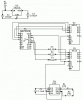
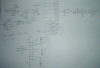
I would like to make one of these effects. They allow you to lower bit rates and alter sampling frequencies of an incoming signal for "lo-fi" type effects. My plan is to use an 8-bit ADC chip, giving a maximum of 8-bit resolution. To alter the bit rate down, I intend to be able to switch out the LSB's with 4066 CMOS switches, I think this would achieve the right effect?

To alter the sampling frequency I plan to have a set of latches on the digital outputs (the 4516 chip using the parellel load feature) which are latched by a variable frequency oscillator. By lowering the oscillator frequency, the number of samples passed per second can be reduced?

The only ADC chip I can get easily is the ADC0804LCN. It seems to be designed to be used with microprocessors, which I don't intend. Is it suitable? Also, the conversion time is a little long at under 100uS, I hope it is under it by a bit, but it shouldn't matter too much.

Looking at the datasheet, page 11's free running connection looks suitable? It generally looks a bit of a hassle to hook up (seperate grounds for analogue and digital?), is there much chance of getting one working (and a breadboard test is required too).
 
I don't do much audio stuff, so it took a while to search for the context. The bit-rate thing should be fine, it's just that 8 bits isn't exactly a lot of headroom to start with and lowering it from there is just going to make it sound even noisier. - Is there any way of simulating this stuff on the computer? I'd assume that there's some sample rate converter that will convert normal quality sound into something that's 8bit/10KHz. As far as I remember though, 8 bit sound is typically put through a compander so that the quieter sounds don't get lost - as it is, I'd guess it's going to sound worse than telephone quality (without the effects)...

The 4516 would let you divide the frequency by 1..15, so it would work if you can feed in a ~10KHz signal.

That mode of the ADC0804 should work, just keep an eye out for the note about the WR pin needing an initial pulse when the ADC is starting up. Alternatively, feed the carry-out of the 4516 into the WR pin and use that to start the conversion.

In order to get the lowest noise, the chip has multiple grounds so that it can isolate the noisy high-speed bus from the analog section. Just connect both of them up to the common ground line.
 
Thanks for the reply. I've tried twice to draw up schematics and given up both times :D

Hadn't thought too much about noise, but that could get a bit excessive. The effect is "grungey", but I don't really disire noise. It kind of simulates old computer sound quality, but is fully variable. I like the way it sounds on drums, snares in particular, it's "crispy" :D. I do have a computer one, VST job, but I want a real one for the "hands on" feel.

The use of the 4516 isn't quite standard. What i'm doing is using thier parellel load feature, they are essentially latches (I may use latches instead, but am familiar with the 4516). By applying pulses to the PL input, the numbers at the input are send out and held until the next pulse, upon which the current number is once again sent to the output and held. By altering the oscillator speed of the pulse source, it is effectively possible to lower the sampling rate? The half drawn schematic may make it clearer (there should be a hpf and schmitt to shorten the 555 output pulses and assume the 555 freq is variable).

I'm not certain I will persue this anyway, it looks a bit of a tricky one to get going and may be dissapointing. What I need is to buy the ADC and experiment on breadboard before buying the case, controls etc, but that way I pay extra postge which annoys me.

I will also require op-amps as buffers and amplifiers on the inputs and outputs and for the R2 DAC. If the chip uses a 5v supply, how should I power the op-amps? Low voltage ones, or run them off of higher voltage and use capacitive coupling? The chip seems to be protected against overvoltage to some degree. The intended power supply is a 12VAC (or 9vac) wall pack with the power supply systems internal.
 

Attachments

  • decimator.gif
    decimator.gif
    6 KB · Views: 580
I was thinking more about quantization noise, but as long as you've simulated this out, that's fine. I think you'll definitely want an adjustable gain on the input in addition to a volume control at the output though.

Oh I see, I thought you wanted to use them as a clock divider... Well, if that's your worry, then you don't even need the 4516's - the ADC has a built in latch that holds the value between conversions. Just start the conversions at whatever rate you want (i.e. fed by the adjustable 555), and just use the D0-D7 pins as is, masking out the lower bits as you see fit.

Capacitive coupling is probably the way to go - have the input and output stages use whatever components you're comfortable with (I have a tendency to use the latest and greatest parts, but costs of the custom boards means I don't build projects too often), and AC couple/divide the signal into the 0-5V range of the ADC (centered around 2.5V), and do the same on the output.
 
Thats good, I can save some board space and effort that way :). What pin will I need to supply the variable clock to though?

I mainly intended on having the level adjustment on the input, possibly on the output too, but the mixer it will be connected to can deal with that probably. Just a simple op-amp amplifier with variable feedback I was thinking.

I would probably have the op-amp on a seperate 12v regulated supply with a potential divider giving a 6v reference/artificial ground, then another voltage divider at the output into the ADC so that the maximum voltage is 5v; although using the artificial 6v reference, I probably need capacitive coupling too? Capacitive coupling on the input too I would think.

My sim would crash and burn simulating anything more complex than a light bulb, so i'll need to do a lot of breadboarding if I do this (probably get 2 ADCs, I can see myself breaking one). Nothing here is too high frequency for breadboard is it? I should learn a bit about ADCs if nothing else!
 
Last edited:
Bear in mind you don't just require buffers on the input and output, you require low-pass filters as well - choose your low-pass filters to be at least 1/3 the sampling frequency, preferably even lower. As you're not doing any processing the sampling frequency can be fairly high anyway, mainly limited by the speed of the A2D.
 
Yeah, I had thought of that, I have a LPF, HPF section on a block diagram a drew. The HPF will likely be taken care of by any capacitive coupling, it's just to remove the DC. I'm still not sure how I set the sampling frequency of that ADC though? Is it via the clock pin, I use an external clock? 10Khz is quite low, and a filter 1/3 of that is a bit too low so hopefully the ADC can run a bit faster if pushed?
 
It looks like it might reach 16Khz if the clock is ran at 1.2Mhz and the chip is supplied from 6V. Is it the clock speed I change to alter the sampling frequency though? It lists a minimum on the datasheet of 100khz, will it fail to work below this? I want to be able to take it under 1khz sampling rate really :D, 100k seems to equate to 1.3k or so (might be alright)
 
Well, the datasheet from Natl. Semi. says that accuracy is guaranteed at sampling frequencies of 10KHz and below, but running it faster makes you lose bits... Thats the effect you wanted anyway isn't it ? *grin*.

When this particular ADC sees a low signal on it's "/WR" pin, it will go into a reset state, and when the pin goes back high, it will start a conversion. Just supply a 10KHz pulse stream with a negative pulse width of >100nsec (but as narrow as possible) into this pin.
 
Ah, good. Didn't like to mess with the clock too much. So I will fix the clock at mabye 800khz, whatever I can get away with :D

The /wr pin is is tied to the /intr pin on the free running mode, I assume I reset them both with the 555 clocking system? And just by varying a 555 frequency, I can effectively change the sampling rate? I'm not certain if that can work. As the /wr pin forces a reset state, say i supplied a low 2khz pulse stream, it wouldn't take 2000samples/s, rather it would be reset 2000 times/s and between each reset will take as many samples as dictated by the clock (mabye 5 in this case)? So it will try to take it's full 10000 samples, but will keep being interupted. Mabye i'm missing something.

Thanks for all your help so far btw, I think I understand it all a bit better now :)
 
Well, if you supply the sampling clock, it's no longer running in "free-running" mode - leave the /intr line open, and just connect the /wr line to the 555. That'll make it take 1 sample/conversion per cycle. The 555 runs at 2KHz, you'll get a 2KHz sampling rate. After the ADC has done it's conversions it'll just sit there waiting for the next /wr pulse.
 
Ah, excellent, I don't fully understand what all the pins do :). So just feed a fixed clock and use /wr to control the sampling rate. /intr is left unconnected. I have a breadboarded CMOS 7555 clock which I can vary from 50khz to 1Mhz, but I probably shan't use it, except mabye to determine the highest operation freq of my chip. I can use the internal clocking scheme.
 
Last edited:
Hello again. I'm having more thoughts about this, and the op-amps. Do you think it would be more suitable to use this:

**broken link removed**

TLC27L4CN

Since it runs from 5v and being CMOS is presumably rail to rail? It should make things easier, providing it is suitable for audio (low noise, distortion?). I would only require a 5v (probably 5.8 in fact) supply altogether if these would work and don't need to worry about clipping signals into the ADC etc so much.

A high (over VDD) signal input voltage wouldn't damage these op-amps would it? I guess protection diodes could be used if there were a chance of it.

Also, how would you connect the input signal, since the op-amp is single supply, connecting between ground and the input would leave a half wave signal. Capacitive coupling, reference the negative input to half supply?
 
Ok, heres a schematic; I finally decided to do it :)

- The input is capacitively coupled, this will pass the full signal with a single supply? It seems to in guitar FX pedals, or does the + input of the inverting amp need to go to 1/2 of V+? Gain can be adjusted with the feedback pot to suit different inputs.

- The sampling rate of the ADC is controlled by the 555 oscillator. It produces short negative pulses required by going through a high pass filter and inverting schmitt trigger (40106 fast enough?). I will find the values for the filter with the scope.

- I want the ADC to run at 750Khz, so need suitable R and C values to do this.

- At the DAC, bits can be discrarded by switching on 4066 bilateral switches (or ordinary MOSFETS?) which ground the 3 LSB's when activated. The 10k resistors stop this presenting a short at the output of the ADC. The switches are activated from a set of comparators controlled by a pot. (oops, the side with all the switches connected should go to 0v)

- A low-pass filter and high pass filter (should be around 6K and 30Hz respectively) are used at the output to remove unwanted harmonics/DC.

As noted, the op-amps are CMOS TLC27L4 which can run from only 5v single supply. I hope these are suitable? Comparators are LM339. The 5.8 supply is higher than 5v to allow the ADC to run a little faster; it will be a fully regulated supply. I haven't shown the parallel digital connection between the ADC and DAC for neatness. Hand drawn since my software doesn't have half the parts and I find it slow to use tbh.
 

Attachments

  • decimator schematic.gif
    decimator schematic.gif
    390.2 KB · Views: 448
The opamps need to be tied to some virtual ground at VCC/2. AC coupling should be fine. I'll let you dig through the ADC data sheet :). The TLC27L4 might not be the best choice - the GBW is pretty low, and it seems to be more meant for instrumentation applications - it seems to be the low power variant of the more common TLC274. If you dig around TI's website you can see all the recent variants of it. In any case, it does use a standard pinout, so later on you can just swap the chip out if it becomes a problem.

Incidentally, about the 4066 switches - the four things you can do with the bits are short the DAC bits to VCC, GND, VCC/2, or just open circuit them. This corresponds to rounding the numbers up, down, towards '0', and truncation (?dunno about the last one). There shouldn't be any difference between the first two, and the last one, but there is a minor difference if you short the DAC lines to VCC/2. I don't know which one you'd like to do though.
 
Thanks for the reply. To provide 1/2vcc (2.9v I guess), a pair of 10k resistors or similar could be used for the input amp and summing amp at least. For the filter though, i'm not sure if that would affect it adversely, being a relatively high impedance ground? The TLE2426 would be ideal, but my supplier doesn't stock it :( . I guess if the high impedance ground is an issue, a ground formed by potential divider but buffered by an op-amp would be more suitable?

EDIT: The LM317LZ 100MA would do by the looks of it if required.

For op-amp's, i'm looking here since this is my normal supplier and I like to use them:

**broken link removed**

If that is the low power version, what are the main drawbacks; apparently the normal one isn't stocked, though the single version is (expensive for 4). What is GBW :eek: ? If you find any other suitable ones available there let me know :) . Requirement is that it is suitable for low voltage, has rail to rail swing (must be CMOS to do so?) and is suitable for audio (fairly low distortion, noise).

How I currently have the 4066's arranged is "shorting" to ground, so the DAC see's 0v on any of the LSBs when activated. I thought it would be bad to directly short, hence the 10k protection? I see what you mean about using 1/2vcc, that may be best, or at least different. Probably will try on breadboard to see.

A couple of other things, is that input to the ADC wired corrently? I couldn't figure it out :eek: . Also, is that 40106 schmitt fast enough to produce 100ns pulses? If not, what might be a suitable gate (don't really need 6 either, lol)

Thanks again :)

EDIT: Perhaps the LMC660CN is more suitable? Didn't realise that was a quad. Has a good output swing and low distortion at least.
 
Last edited:
A standard voltage regulator is a bad idea since they usually can't sink current. The standard approach is to use a free opamp to buffer the voltage coming out of a resistive divider. If you have can burn some power (by reducing the resistor values of the divider to much less(say an order of magnitude or two) than any loads connected), and can put enough capacitance on the line, it would be good enough. The ADC0804 has a Vref impedance of ~1K, so this is probably the limiting factor.

Since you seem to be using all the opamps, one substution would be to just use another quad opamp instead of the comparators, and use the one remaining opamp as the mid-rail buffer.

GBW is the gain * bandwidth product. If you have an opamp with a GBW of 1.4, you can build a unit gain amplifier that can work with 1.4MHz signals. If you have a gain of 10, then it can only support .14MHz signals, and so on. The other number you tend to look at is slew-rate, and occasionally phase margin. The slew rate tells you how fast of a signal the opamp can support without distorting it - a 10V sine wave has 10x the slew rate of a 1V sine wave, so it inherently tells you how big of a signal the opamp can output. (I haven't done any opamp circuits lately, so I might be a bit off).

The LMC660 should work fine (the TLC274L4 wouldn't have any problems either). In any case, both these opamps won't work with the positive rail - most of the newer opamps - (i.e. ones that have been designed in the last 5-10 years) do rail-to-rail input and output. These two particlar ones only go up 2V of the upper rail - the largest signal that you'll want to feed into these opamps is ~3V considering the 5V rail voltage. It might make sense to
1) set the virtual ground at 1.5V
2) set the ADC0802's Vref/2 to the same voltage
3) or just supply the opamps with some higher voltage and leave everything at VCC/2

Signal is connected to V+ input, ground connected to V-, seems okay.

The inverter probably isn't fast enough to do 100ns pulses, but it probably isn't needed in the first place. The main reason for making the negative pulse as short as possible is to get higher bit rates... bleh, resuscitating my 555 skillz... Is there any reason for having the adjustable resistor on the 555 on the discharge path? To generate a very short negative pulse, I'd try to put a small fixed value for "Rb", and use the variable resistor for "Ra"
 
Thanks for the reply again :)

Ok, i'll avoid the voltage regulator. I think even a high impedance 1/2vcc will be ok (2x10k resistors) if I just change that low pass filter for a passive one and buffer (as per the HPF)? That way, only refrences are required, not current paths, I think.

Right, I understand the GBW now. Should be fine for audio like this since no gain will be especially high (line or guitar in, not mic).

I'm concerned about them not being rail-to-rail? I looked at the dataheet and gathered it will go within 0.24v of the positive rail. I've attached what i'm looking at in case i'm missing something. Perhaps the input limits it, not the output?

I think i'd rather use a faster schmitt invertor, the 555 resistors never seem very independant of each other. In actual fact, i'd most like to change the 555 for a VCO of some sort (if this works at all); probably the LM331? That way it can all be voltage controlled by an interface if desired. The 74HC14 might be fast enough?
 

Attachments

  • op-amp swing.gif
    op-amp swing.gif
    47.2 KB · Views: 318
The issue is that the ADC requires a relatively low impedance (~1K) on it's Vref input - which happens to be VCC/2 = the virtual ground rail. Other than that, the only other place is one of the nodes from the opamps, and that one is connected in series with a 22K resistor...

The input of the opamp is the problem. Pushing any voltage above the recommended input maximum does strange things - gain goes nutty, and occasionally negative.

Well, I think swapping the variable resistor location is the way to go - along with having a 100 Ohm or so resistor as the discharge one. The pot. then adjusts the high time which corresponds to the when the converter is actually converting. In any case, it's not exactly important which way this gets implemented since this isn't in the signal path.

HC logic parts should be fast enough.
 
Thanks :) . Ok, I think this is how i'll do it;

I'll use the 1.5v "ground", and reference vref2 of the ADC to 1.5v also (though with a 5.8v supply, perhaps that should be a 1.9v ref?). This way the ADC gives a full digital output from 0-256 with a voltage at the input varying from 0-3v? Leaves a small headroom, but should be ok with input gain control.

I'll use the LMC660. I'll be able to free one up for the 1.5v (1.9?) reference by using two passive filters in a row instead, followed by a buffer or possibly adjustable output amplifier.

I'll probably try to use the LM331 VCO with the HC schmitt to produce short pulses. That way I can control the "sampling rate" by an external voltage control. The bit depth is already voltage controllable. Should be fun with a MIDI-CV convertor if I ever get one :)

I calculate the C and R for the ADC clock to be suitable as 22pF and around 50k. Gives a fairly high clock frequency which I hope it can deal with because of the extra supply voltage. Plus I already have 22pF polystyrence caps :)

I better order some bits soon, quite a lot of moderately expensive chips required. Might make changes when I see the results on breadboard (if it does anything at all, lol).

Thanks again :)
 
Status
Not open for further replies.

Latest threads

New Articles From Microcontroller Tips

Back
Top