Continue to Site

Welcome to our site!

Electro Tech is an online community (with over 170,000 members) who enjoy talking about and building electronic circuits, projects and gadgets. To participate you need to register. Registration is free. Click here to register now.

  • Welcome to our site! Electro Tech is an online community (with over 170,000 members) who enjoy talking about and building electronic circuits, projects and gadgets. To participate you need to register. Registration is free. Click here to register now.
Status
Not open for further replies.

mading2018

Member
Hello,

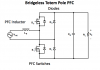
I used the LT8312 PFC controller to controlling the switches, but somehow the switches seems not to operating in the bridge, only the diodes.
Do anyone know what could be the problem why the switches do not operate?

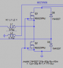
And how do I change the switching frequency to 150 kHz? I think that I should you use this equation: f_c = 1/(2 pi R C)
in order to calculate the values for C3 or R12 at the DCM. What I understand from the document the f_c needs to be lower than 12 Hz.

PS. However, it feels like the time period of the output of one waveform period is always 10ms, so it means I have 100 Hz as switching freq, even tough I tried to change the C3 and R12 DS.

The LT8312 have max switching frequency of 400 kHz according to data sheet.

Thank you all,

mading
 

Attachments

  • OFF_ACDC_Totempole_PFC.asc
    7.9 KB · Views: 280
Last edited:
I did used the demo for LT8312 in this circuit, I just modified to make a totem-pole, where there are two switches connected. Like this I have attached.

I saw one misstake in my circuit now, I have connected the AC side wrong to the bridge, I have adjusted it now.
 

Attachments

  • totem.png
    totem.png
    39.8 KB · Views: 244
  • OFF_ACDC_Totempole_PFC.asc
    8 KB · Views: 233
The all MOSFETs are turned on with a voltage from G to S, NOT from Gate to ground.
The source of S2 is not at ground. It can not be controlled by an IC that is sitting on ground.
upload_2018-4-12_8-36-9.png

And you never made this circuit.
And this is not "interleaved".
 
Post #4 circuit 2. Q3 shorted G-S. Q2 shorted G-D.
Post #4 circuit 2 & 3. What is in red below is not in circuit 2 & 3. You have the right side of Lb connected to S2 Drain.
upload_2018-4-12_9-1-58.png
 
Red circle. Q3 gate shorted to ground. Q2 gate shorted shorted to ground.
Blue circle. You can not drive Q3 gate directly from the IC.
upload_2018-4-12_9-25-45.png
 
Red circle. Q3 gate shorted to ground. Q2 gate shorted shorted to ground.
Blue circle. You can not drive Q3 gate directly from the IC.
View attachment 112263

Okay, I see. But how can I create an voltage over the gate and source for Q2 and Q3 with the IC? By adding a voltage source as we did for the switches for the DC/DC converter?

You say that I can't drive Q3 gate directly from the IC, where should the gate of Q3 be connected to in that case? I am not sure..
 
Probably one of the most used parts to drive "high side MOSFETs" is the IRS2004.
It is built to drive both high and low side FETs.

This version of PFC with two MOSFETs is complicated.
 
Probably one of the most used parts to drive "high side MOSFETs" is the IRS2004.
It is built to drive both high and low side FETs.

This version of PFC with two MOSFETs is complicated.
Hmm, I tried to look for the MOSFET IRS2004 in LTspice but I couldn't find that part in library.

What do you suggest that I can do to make this work? Cause I don't know what I should do next.
 
Last edited:
In SPICE use a voltage controlled voltage source to get isolation.
This you tube is slow and hard to hear but try it.

Here is a VCVS. In this case the voltage on the inputs is goes through a formula then to the output.
Vin X 50 = Vout
In your case change 50 to 1.
The output of a IC can connect to the input of the VCVS. (also ground)
The MOSFET (that is not on ground ) connect Gate to (+) and Source to (-).
The right hand GND could be anything, because there is isolation inside the VCVS.
upload_2018-4-13_7-20-4.jpeg
 
Hmm, I am not sure if I understand the connections parts. I tried to follow your comments.
Maybe its better if you can edit my file, it will be clearer I think.

Here is my attempt, see the attached file.

I changed now to LT1249 instead, cause its operating for CCM (what I want since my calculations are based on CCM) and fixed 100 kHz (closed to 150 kHz).
 

Attachments

  • LT1249_TA01 (3).asc
    6.6 KB · Views: 213
Last edited:
The idea is to take the bottom MOSFET gate signal and invert it. So I set the gain of E1 to -1. The (-) inverts the signal.
I could not find a way to subtract 13 volts from the signal so I set E1 on a 13V voltage source.
If you plat GTDR and compare to Q3GATE-Q3SOURCE you will see that any time Q2 is on Q1 is not on.
upload_2018-4-14_8-26-17.png

Your circuit is not working. I don't know what it should do.
I just fixed the top MOSFET gate drive problem.
 

Attachments

  • LT1249_TA01 (3)-ron-x.asc
    6.1 KB · Views: 215
Aha, I see. thank you.
The idea with this circuit is to get convert the incoming AC voltage (from the grid) to an DC voltage (like an AC/DC converter with boost PFC),
and having a Totem-pole PFC for this one instead.
 
Aha, I see. thank you.
The idea with this circuit is to get convert the incoming AC voltage (from the grid) to an DC voltage (like an AC/DC converter with boost PFC),
and having a Totem-pole PFC for this one instead.
I know but its not working. Maybe the two Gate signals are not right. Where did you get this idea? They should give you information on when the top switch should be on and when the bottom switch should be on. It is easy to say "here is a circuit" and "magic drives the two switches". Many books show a circuit + magic. (never been tried)
 
I got this idea cause it is using less components, thus the charger could possibly be smaller.
https://www.kivi.nl/uploads/media/59565ab464588/Guido-Schott.pdf

I think the duty cycle should be 0.19 according to my calculations, but how can that be implemented in the circuit?
Its says according to this source that I have used: "D is the duty ratio of the active switch (Q1 or Q2) of the fast switching leg."
https://unitedsic.com/wp-content/uploads/2017/06/Totem-Pole-PFC-v2-AppNote-2017-06-23.pdf
 
I got this idea cause it is using less components, thus the charger could possibly be smaller.
Driving the top MOSFET adds a 8-pin IC and parts.
I do like the idea of not having fast diodes. (using a MOSFET as a fast diode) I do not see how it is smaller.
https://www.kivi.nl/uploads/media/59565ab464588/Guido-Schott.pdf
This only shows a thought. It does not show how to do it. I think Guido Schott never built one. He does not know how.

I think the duty cycle should be 0.19 according
The duty cycle changes. Line voltage 0/360V/0/-360/0........ The duty cycle changes with the line voltage. I think "0.19" is at +360V or -360V. At 50V the duty cycle is different.
----edited----
You must not allow both MOSFETS to be on at the same time. (more parts)
 
Status
Not open for further replies.

Latest threads

New Articles From Microcontroller Tips

Back
Top