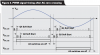
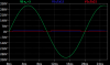
It should alter I think, first Q1 is ON, where Ton should be much longer (long enough to be on during the positive side of the AC voltage waveform), and
than Q2 is ON (Q1 OFF), long enough to be on during the negative side of the AC voltage waveform.
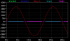
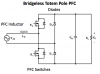
Yes I have read it, but since it is complex for me to understand, I am trying to obtain Q1 and Q2 only and not Q3 and Q4. (I also have only Q1 and Q2 in my topology).


") .
.