Electro Tech is an online community (with over 170,000 members) who enjoy talking about and building electronic circuits, projects and gadgets. To participate you need to register. Registration is free. Click here to register now.
Welcome to our site! Electro Tech is an online community (with over 170,000 members) who enjoy talking about and building electronic circuits, projects and gadgets. To participate you need to register. Registration is free. Click here to register now.
I use them, usually the single ended ones - I would suggest you get a track cutting tool as well - for years (decades) I used a twist drill in my fingers, and it's SO MUCH EASIER to use the proper tool
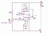
Remember you are working with millivolt level ac signals.
You must keep the interconnecting wires as short as 'reasonable' else you will pick up mains em radiation which will give reading errors.
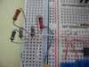
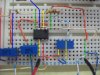
I would recommend that you build the CA3140 amplifier, this will increase the voltage that is output from the AD736.
You can use your dc meter to check the output.
Use a pot about 10k or 20K as a test input source for the amplifier.
hi,
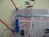
If I am reading your post correctly, you are saying you havn't adjusted the 20K pot.???
You need to turn the pot to give a 'X' point voltage of 1Volt [use a small screwdriver]
Once you have set 'X' at 1V then adjust the gain pot to give +3V on the output of the CA3140 'Y'.
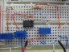
Read the instruction notes on the drawing.
The term 'SET' means adjust.
The VR1 pot has been adjusted to give 1.08VDC I could try and fine tune it further to give 1 VDC exactly.
The gain pot becuase it is shorted if I tun it to one side it will go below 2.86 VDC and if I turn it to the other and once it passes the centre point it never goes beyond 2.86 VDC.
The only pot I have not adjusted is the one connecting 1 to 5.
I assumed those figures are sort of correct with a certain margin of error or I am wrong?
h
If I am reading your post correctly, you are saying you havn't adjusted the 20K pot.???
You need to turn the pot to give a 'X' point voltage of 1Volt [use a small screwdriver]
Once you have set 'X' at 1V then adjust the gain pot to give +3V on the output of the CA3140 'Y'.
Read the instruction notes on the drawing.
The term 'SET' means adjust.
The VR1 pot has been adjusted to give 1.08VDC I could try and fine tune it further to give 1 VDC exactly.
The gain pot becuase it is shorted if I tun it to one side it will go below 2.86 VDC and if I turn it to the other and once it passes the centre point it never goes beyond 2.86 VDC.
The only pot I have not adjusted is the one connecting 1 to 5.
I assumed those figures are sort of correct with a certain margin of error or I am wrong?
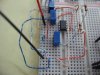
The VR2 pot is not shorted.
You should be able to set the VR2 gain pot from 1 thru times 4
So the output pin should read from about 1V thru 4V as you adjust VR2.
The VR2 pot is not shorted.
You should be able to set the VR2 gain pot from 1 thru times 4
So the output pin should read from about 1V thru 4V as you adjust VR2.
For a test remove the 10K pot between pin 1 and 5 [ leave the wire links in place], leave it out for now.
I assume the the +V is 5Volts.
Try adjusting VR1 and measure the X and Y voltages, just do about 5 readings from say X = 0, 0.2, 0.5, 1.0, 1.5V
As close as you can get, its difficult with a single turn pot, lets know the Y voltages.
This site uses cookies to help personalise content, tailor your experience and to keep you logged in if you register.
By continuing to use this site, you are consenting to our use of cookies.