mading2018
Member
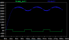
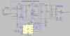
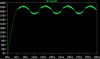
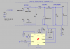
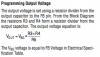
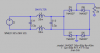
For the C2, C4 and R3 are standard values from a demo for the LT1249, so I haven't change them yet. Yes, it would be great if you have some time to fix it as soonest you have time. Thank you very much, appreciate all your help.Your full wave bridge is not working. Remove the ground with the red X.
I do not know why R1.
View attachment 112031
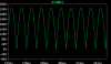
It is not working right. It looks like the frequency response of the error amp is not right. C2,4, R3.
I don't have time to fix it today.