Continue to Site

Welcome to our site!

Electro Tech is an online community (with over 170,000 members) who enjoy talking about and building electronic circuits, projects and gadgets. To participate you need to register. Registration is free. Click here to register now.

  • Welcome to our site! Electro Tech is an online community (with over 170,000 members) who enjoy talking about and building electronic circuits, projects and gadgets. To participate you need to register. Registration is free. Click here to register now.

LED Strip lights (2 Amps) Short Fade on / Fade Off effect

Status
Not open for further replies.
Condensed Schematic. Relay connected wrong
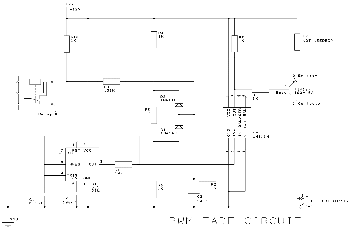
FadePWM - Project-1.png
 
I think you have a double inversion now; for low=on, either swapping the 311 inputs or using a PNP output; not both.
 
One simple way, use ATTINY85 to do supply sensing and PWM generation.

Here is a block programed partial solution that does both ramps. Note it can
easily be modified to handle a brownout type situation if you care about that.

mBlock takes the blocks you config and generates the Arduino code for you.

Current functionality is on power on a ramp up is done. Then if ATTINY85 detects
10 V from a 1/4 voltage divider external then a ramp down is performed.
Solution then stays in do nothing loop until power is lost and ATTINY85 restarts.
You can change the 10V to whatever you consider loss of power V should be.

Design should power up with no funky artifacts as ATTINY85 power up is well
controlled internally. I would add a 10K R from Darlington base to ground to
absorb leakage when Darlington is supposed to be off. For startup considerations
when ATTINY85 I/O pin is in no mans land for first couple of volts. and then it starts up
as input until program takes over and forces it as output logic 0. Note if you used
a logic level MOSFET with a threshold around 3 - 4 V that would be better to insure
no false turn on occurs.

1640009988629.png


You would need a nano or uno board to program the ATTINY85, and ATTINY85, a bypass cap
for it, 2 R;s to do a 1/4 V divider for power sensing, and the power interface to LED string, eg.
the Darlington. Timing accuracy much better that 555 timer, including T and V effects.

The ATTINY85 would need a 3 term TO92 V regulator, as that acts also as Vref for A/D in this example.
A 2% part would be a better Vref than its onboard Vref. or a shunt zener with tight tolerance for a
regulator.


iu


Project attached. Use mBlock 5.3.5 to open.


Regards, Dana.
 

Attachments

  • Ramp Up andDown LED String.zip
    55.5 KB · Views: 183
Last edited:
One simple way, use ATTINY85 to do supply sensing and PWM generation.
I can recognize some of the routines and variable declarations from my programming days. The compact design of the hardware makes for a very small footprint. Something i like.
 
Yep, it was for the single LED.
If the LED lamp you are using is designed for direct 12V connection, you do not need that resistor, just link it out or remove it.
 
hi

If you replace the relay contact with the output of a second 555, the circuit could be made to alternately fade/on and fade/off automatically.
 
hi

If you replace the relay contact with the output of a second 555, the circuit could be made to alternately fade/on and fade/off automatically.
i don't follow you. curious...
when the relay is closed the light fades on and when it opens the light fades off. what would be automatically done.
 
It looks reasonable circuit-wise, my main comments are:

Do not use thin tracks when there is no good reason you cannot use thicker ones; especially such the power track through to the light output and the light negative to the transistor - that small track is likely to act as a fuse! Every track on on the board could be the same width as the existing power tracks, and power rather wider.

And as it's double sided anyway, make the top side a ground plane; again, there is no reason not to, and it eliminates ground track width problems.

Also, you have the power track doing a complete lap around the board then passing itself against the "NE555" text, rather than being connected to give alternate current paths?

I just realised - if that's EasyEDA, the layers are reversed? For conventional components (rather than surface mount), the general interconnections should be on the solder side of the PCB and ground plane on the component side?

IMG_5646.jpgIMG_5647.jpg

[Just realised that board has not been de-fluxed yet :rolleyes: ]
 
make the top side a ground plane; again, there is no reason not to, and it eliminates ground track width problems.
ok done. i do have top and bottom ground planes. just took them off to show the tracks. DS obscures the tracks after their poured.
If I make the tracks any wider than 25 i get drill errors in the design check. ive read that it is ok (old tech) but ive also read that its not.
pmw fade ver1.1.png
 
i don't follow you. curious...
when the relay is closed the light fades on and when it opens the light fades off. what would be automatically done.

Currently, the LED(s) will fade on, then remain on as long the relay is energized. The LED(s) will fade off, then remain off when the relay is de-energized. Maybe that is the operation you want. If so, ignore the following comments.

I just thought I'd mention that with an additional 555 output replacing the relay contact, the circuit could be made to continuously fade-on and fade-off automatically by a single switch closure or when the additional 555 powers on. You wouldn't have to manually initiate a fade-on or a fade-off.
 
ok done. i do have top and bottom ground planes. just took them off to show the tracks. DS obscures the tracks after their poured.
If I make the tracks any wider than 25 i get drill errors in the design check. ive read that it is ok (old tech) but ive also read that its not.View attachment 135218

The only place where beefy traces are needed is at the collector and emitter of the Darlington transistor, as well as the PWR input.
Emitter is probably connected to the ground plane, so that's good. But the collector track is carrying alot of current so should be wide. The PWR track from the power input (wherever that is) to the light could be a small copper plane on the top side.
 
The PWR track from the power input (wherever that is) to the light could be a small copper plane on the top side.
a small copper plane? like a copper shape that i add (not to the entire board) then pour? Id like to do this. How?
 
Just trying this out.
I replaced the full top copper pour GND with 2 polygon areas. the lower is a top pour for 12V and the upper area (remainder) is a GND pour.
This is to give as much copper as possible to the important areas. did I get this correct?
pmw fade ver1.1 Copper Pour.png

NOTE: I left out the bottom pour (GND) so you can see the top pour.
 
Just trying this out.
I replaced the full top copper pour GND with 2 polygon areas. the lower is a top pour for 12V and the upper area (remainder) is a GND pour.
This is to give as much copper as possible to the important areas. did I get this correct?
View attachment 135219
NOTE: I left out the bottom pour (GND) so you can see the top pour.

Yup...that's the basic idea. But be sure to not leave any isolated planes like at the top right corner area. The planes should be joined with their appropriate copper sections. So you'll end up with two contiguous upper planes, one for GND and one for 12v.
 
Status
Not open for further replies.

Latest threads

New Articles From Microcontroller Tips

Back
Top