Continue to Site

Welcome to our site!

Electro Tech is an online community (with over 170,000 members) who enjoy talking about and building electronic circuits, projects and gadgets. To participate you need to register. Registration is free. Click here to register now.

  • Welcome to our site! Electro Tech is an online community (with over 170,000 members) who enjoy talking about and building electronic circuits, projects and gadgets. To participate you need to register. Registration is free. Click here to register now.

SC8560 AM/FM clock radio 50Hz drifts

Status
Not open for further replies.
Hero999
May be you missed my latest post. Here i am again.
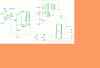
I did try using the RC filter and it did not help.

Here is what the data sheet says for the voltage levels
Input "H" level voltage --- Minimum -1v
Input "L" level voltage --- Max Vdd+2 volts.
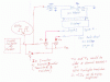
 
You should post your circuit. It is tedious for me and presumably the others to have to read through your verbal descriptions.
 
Folks
Apologies for not uploading the schematic. I was trying to draw it again ( dont have a scanner handy).

I am uploading the 60Hz-circuit.gif file.

I have tried following too
-- Instead of C5, i have used a low pass filter, It did not help
-- I was slightly confused with using the Vdd/Vss from 8560 and reverse connecting it to Vdd/Vss of the CD4XXX circuit, so I tried to use a separate power supply for the CD4XXX and to be on the safer side, used a optoisolator MCT2E to couple 60Hz signal so that i am sure the powersupplies are totally isolate. But that did not help too !!

I think the problem is now related to the multiplexing of the LED's. continous counting may be that I am using a 60Hz timing reference, but the IC is wired to use the 50Hz from the transformer to multiplexing the LEDs. (This is what even some of the google groups posting replies indicate toooo)
 

Attachments

  • 60Hz-Circuit-1.GIF
    60Hz-Circuit-1.GIF
    13.5 KB · Views: 881
Last edited:
What's the value of C5?

Have you tried adding a pull-up/down resistor on pin 25?
 
Thanks for posting your circuit, now we can see what you are doing.

Several points are immediately obvious.

1. The counters are being reset after the delays due to C1/R1 & C2/R2. As I told you in a previous post, you don't need to reset the counters in this case since you are using them as frequency dividers. Connect the reset pins on both counters to Vss.

2. I don't understand why you have reversed Vss and Vdd for the SC8560. But I have not looked at its data sheet yet. Don't have one. I'll download one later.

3. You have capacitively coupled the SC8560 via C5 but do not have a pull down resistor on SC8560/pin 25.

I have attached a positive version of your circuit as I found the negative one tedious to look at.

EDIT. I downloaded the data sheet of the SC8560. Now I understand why you had to transpose Vdd & Vss. However, you don't need C5. Just connect it directly.
 

Attachments

  • 60Hz-Circuit-2.GIF
    60Hz-Circuit-2.GIF
    13.5 KB · Views: 1,100
Last edited:
The Oriental clock IC maker has the terms Vss and Vcc mixed up.
Maybe this new counter cicrcuit needs its own supply bypass capacitors.
 
audioguru said:
The Oriental clock IC maker has the terms Vss and Vcc mixed up.
Maybe this new counter cicrcuit needs its own supply bypass capacitors.
No, it is a P MOS device hence Vdd is negative wrt Vss.

Yes, I forgot this point. He needs 100 nF between Vss and Vdd on each IC.
 
Folks,
Thanks for all the help. But none of the tips help !!! I tried removing C5 and adding 100nf bypass capacitors !!!
As i have posted earlier, i tried separate power supplier and connecting the CMOS circuit via an optoisolator pair to the clock IC just to isolate any wierd powersupply etc related problems !!!!

Merry Christmas and wish u all a very happy new year and great vacation !!
 
manoj.patil.1974 said:
Folks,
Thanks for all the help. But none of the tips help !!! I tried removing C5 and adding 100nf bypass capacitors ........... CMOS circuit via an optoisolator pair to the clock IC just to isolate any wierd powersupply etc related problems ............. QUOTE]

Hi Manoj,
1. Did you go thro'my mail
2. Is the circuit almost similar to the datasheet circuit.( ther are 2 circuits there. -- one with +ve voltage and other with negative voltage working. --which one your clock followed. --i do understand the VDD Vss voltage supply reversal issue-- it is correct. that VDD is -ve here.
3. we have now to go deep into the ic details, whether the Display dring 60/ 50 Hz and clock counting 60 / 50 HX should be synchronous?? to be studied with ref to the datasheet.

it is delay and testing patience. continue analysis.it is only for experience not for a clock afterall.
All the best.
 
manoj.patil.1974 said:
Folks,
Thanks for all the help. But none of the tips help !!! I tried removing C5 and adding 100nf bypass capacitors !!!
It is difficult to know, from this distance, what your problem is. So forgive me if I ask some questions that may be obvious.
1. Do you see 600 Hz at IC1 pin 1??

2. If you remove the connection between IC2 and IC3, do you see 60 Hz on pin 13 of IC3?

3. Does the clock work by itself, ie. if you connect a 60 Hz signal (generated by an oscillator of some kind or derived from the mains) to IC3 pin 25?

I know that these questions were covered in earlier posts, but something may have changed.

Also, as someone else implied, the fact that the LEDs are being multiplexed by "50 Hz" and the frequency input is 60 Hz, then this may be a problem since we don't know how the SC8560 works internally.

manoj.patil.1974 said:
As i have posted earlier, i tried separate power supplier and connecting the CMOS circuit via an optoisolator pair to the clock IC just to isolate any wierd powersupply etc related problems !!!!
This should have worked if you did it correctly unlesss the 50 Hz / 60 Hz issue that I alluded to above is the problem.
 
Last edited:
I have thought further about your problem. I think the key is in one of your previous posts.

manoj.patil.1974 said:
However, my larger problem persists. I have connected the CD4060 and CD4018 for power from the SC8560 power supply itself. But, when i connect the 60Hz output of CD4018 to SC8560, it goes into a flickering on LED as if its counting at a very high speed.

So I feel it is a muxing problem caused by the fact that you have a 60 Hz signal from the crystal circuit but the 7 seg displays are being muxed at the 49 Hz rate. But even if you altered the crystal circuit to output 50 Hz, it would not fully solve the problem since there will be a significant phase shift between the 50 Hz and the mains. This will "scramble" the display, ie. cause the "flickering of the LEDs as if its counting at a very high speed"

I looked at the data sheet which is headed:- Silan Semiconductor SC8560", do you have this document?
The block diagram on page 2 and the parameter tables are rather vague about the muxing and it is a strange arrangement.

I expect that you will have to derive the Mux driving signals {currently derived via D3 and D4 (see below)} from the same signal that is connected to pin 25, ie. the output of IC2. I'll help you design a suitable circuit if you answer my questions and confirm that my assumptions above & below are correct.

I assume that your circuit is similar to the diagram on page 8. Is this true?

If so, note that there is an error in this diagram. If you number the diodes D1 ~ D4 from top to bottom, the cathode of D2 (shown conneted to the junction of the 100 k & the 0.001 uF) is connected to the wrong point. It should be connected to the other end of the 100 k, ie. to the transformer secondary.
 
Last edited:
Hi Manoj,
Yes Ijcox has a point.

After seeing the internal schematic of the IC is clear that it is not possible to run the clock from an external 50/60 HZ like the one you derived while the display refeshing (cycle1 and cycle 2) from 50/60Hz of public mains.

These two must be synchronus-- otherwise when a particular disply section is being enabled by internal circuitry meant for cycle 1 the common cathode drive for the concerned set need not aways be enabled, so on so forth.

Now the only way for this is to see that the clocked derived by you shall also have normal and inverted driving power transistors whose output will be fed to cycle1 and cycle 2 points of the display.

Thereafter you don't need to use the tranformer windings meant for this purpose. Hence you can very well convert it to full wave and filter it and use the DC as supply . thus the counting clock and display cycle 1 and cycle 2 clocks will all run from the same derived clock.

Another issue, the IC should not see PF condition . Virtually you are making the clock wok from a battery floated from DC from mains.

regards
 
Last edited:
Hello Big Guys!

this is exactly the same problem i too am facing,

i built the Digi-Clock from Sratch using SC8560, mains freq was inaccurate,

so i made an 50Hz Oscillator using 3.2786MHz Crys +CD4060+CD4013 and connected to the 50Hz input of clock,

the Timekeeping is accurate but the Duplex LED Display displays unwanted segments for one second and next second displays correct time.

there seems to be sync.problem with both 50Hz(Crystal derived) and Mains Freq.

i thought of two options for solving this Problem:

1) make a small inverter operating at Accurate 50Hz(Using Crystal) and feed this 230V AC to the Main supply of the Clock.

2) Eliminate the trafo and make the Clock and Display work on DC using Mosfets for switching.

i tried to replace the two diodes at the trafo with two transistors swtiching at 50Hz (Push-Pull) but the display shows 1P:03 etc.

need some expert help here, this Mux is eating my brains

and also whether the centertap should to be connected to GND or Positive (incase of DC operation)

arun
 
nura100 said:
.................

i thought of two options for solving this Problem:

................
2) Eliminate the trafo and make the Clock and Display work on DC using Mosfets for switching.

i tried to replace the two diodes at the trafo with two transistors swtiching at 50Hz (Push-Pull) but the display shows 1P:03 etc.

need some expert help here, this Mux is eating my brains

and also whether the centertap should to be connected to GND or Positive (incase of DC operation)

arun

Hi Arun,

you try to drive the transistors with the derived crystal clock for cycle 1 and inverted crystal clock for cycle 2.

if still problem, then interchange the cycle 1 and cycle 2 transistor inputs.

the trafo output can safely be used by commoning the anodes of diodes and witha filter condensor,as supply for the disply drive trasistors under reference, instead of using the halfwave rectified supply and trying to load it .

pl leave a feedback

All the best
 
mvs sarma said:
Hi Arun,

you try to drive the transistors with the derived crystal clock for cycle 1 and inverted crystal clock for cycle 2.
This what I'm planning to do. I have been waiting for a respose from Manjo and I was intending to ask him to measure the transformer voltage. But he has not responded yet.

There are several ways that it can be done. Some examples:-

1. Install 2 MOSFET transistors and Zener diodes to limit the voltage to ensure that the display brightness is correct.

2. Use 2 Darlington transistors and 2 Zener diodes.

In each option, the inversion can be done either with an IC inverter or a small signal NPN transistor.

I am happy to design this for you all, but I need to know the AC voltage (RMS) of the transformer winding that supplies the "Cycle 1 & Cycle 2" signals, ie. measure from the centre tap to one of the diode cathodes.
mvs sarma said:
if still problem, then interchange the cycle 1 and cycle 2 transistor inputs.
That should not be necessary as I think I can work out which signal needs to be inverted.
mvs sarma said:
the trafo output can safely be used by commoning the anodes of diodes and witha filter condensor,as supply for the disply drive trasistors under reference, instead of using the halfwave rectified supply and trying to load it .
What do you mean by "the trafo output"?

EDIT. See the other thread in the "Data sheets/parts requests" forum.

EDIT 2. I have attached an outline of one possible solution.

EDIT 3. I have made minor improvements
 

Attachments

  • Improved circuit.gif
    Improved circuit.gif
    31.3 KB · Views: 970
Last edited:
Hi,

Trafo output:- the output of the centre tapped winding -presently used as independent halfwave rectified and each halfwave synchronous to the clockpulse from mains at pin25.

the Dc derived and fed as Vdd will nt be able to drive the displays to the required extent-- theryby need for using the centre tap winding as fullwave rectifier with a suitable filter and then use it as supply to be clocked by derived clock to generate cycle1 and cycle2 synchronous to derived clock.

i am yet to analyze your suggested modif fully except the load requrement of Vdd.this aspect i have already indicated.

good development ljcox,

regards
 
Hello Friends

i already have used the method suggested by ljcox in his diagram, but it doesn't work, when the sources of both the Mosfets are connected to VDD, the display shows some weird symbols which are undesired.
by the way my CD4013's Q & Q- outputs drive two gates of mosfets @ 50Hz

at the first glance it looks very simple to do away with the Trafo and replace with Push-Pull Transistors,

it is not mere swtiching of the Transistors alternately that will solve this problem

but if we have to imitate the Center Tap Trafo, i think we may have to use a
H-Bridge Setup to convert Battery DC into AC

How about a DC-DC converter using CD4093 for Driving PMOS Clock IC?

ljcox your thought on this

nura
 
nura100 said:
Hello Friends

i already have used the method suggested by ljcox in his diagram, but it doesn't work, when the sources of both the Mosfets are connected to VDD, the display shows some weird symbols which are undesired.
by the way my CD4013's Q & Q- outputs drive two gates of mosfets @ 50Hz

...................
nura
Hi Arun, Please try attached diagram.
 
Last edited:
nura100 said:
Hello Friends

i already have used the method suggested by ljcox in his diagram, but it doesn't work, when the sources of both the Mosfets are connected to VDD, the display shows some weird symbols which are undesired.
by the way my CD4013's Q & Q- outputs drive two gates of mosfets @ 50Hz

at the first glance it looks very simple to do away with the Trafo and replace with Push-Pull Transistors,

it is not mere swtiching of the Transistors alternately that will solve this problem

but if we have to imitate the Center Tap Trafo, i think we may have to use a
H-Bridge Setup to convert Battery DC into AC

How about a DC-DC converter using CD4093 for Driving PMOS Clock IC?

ljcox your thought on this

nura
I had not thought that the Vdd supply voltage would not be adequate to supply the display, but, in the original arrangement, obviously the energy comes from the transformer.

I don't understand why you would need a H bridge.

The use of a 4013 to generate anti phase signals is a good idea.

The circuit posted above by sarma looks good to me. I assume Q1 & Q2 are Darlingtons.

Is 330 Ohm sufficient for R3 & R4 given that the supply is now rectified rather than half wave sine pulses?
 
Last edited:
Status
Not open for further replies.

Latest threads

Back
Top