Continue to Site

Welcome to our site!

Electro Tech is an online community (with over 170,000 members) who enjoy talking about and building electronic circuits, projects and gadgets. To participate you need to register. Registration is free. Click here to register now.

  • Welcome to our site! Electro Tech is an online community (with over 170,000 members) who enjoy talking about and building electronic circuits, projects and gadgets. To participate you need to register. Registration is free. Click here to register now.

Pulse Delay?

Status
Not open for further replies.

stizzswizz

New Member
Hello,

I have been working on a this circuit for a while now and I am having some issues with timing.

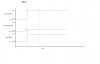
Basically I have to make a circuit to trigger a secondary circuit that ignites a plasma. This is for a PECVD system where I work (semicondutor research center). The system sends out 2 signals that I need to use. One is a 15VDC signal telling me that the system wants the plasma turned on. The second signal is a 0-15VDC RF Power setpoint signal, (0V is 0W and 15V is 300W) I only want my circuit to output 15VDC when the 'plasma on' signal is 15V and the power setpoint is below ~3.0V (~10W). I have built a couple circuits that used opamps, setup as voltage comparators and with bench testing they worked great! However, when installed in the PECVD system, it worked good only when the power setpoint was below 10W. When the power setpoint was say...20W the circuit would output 15V for a fraction of a second. That fraction of a second triggered the ignitor when I didnt want to use it. The problem here is the plasma on signal goes high at like a 1/4 of a second (probably faster) faster than when the power setpoint is reached. I would like to isolate both signals as best as I can (via opto-couplers), and provide around a 300mW output to the secondary circuit.

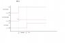
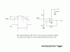
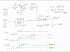
I have currently been trying to use 555 timers to create a single pulse from the plasma on signal, take that pulse and delay it about 1/2 a second. The problem with the 555 that I have is that the plasma on signal is longer then the pulse so it keeps triggering. I have searched online and read alot in my text books on how to make a single shot circuit and it seems like it might work if I can make it auto-reset after a short period of time (1 sec?). I havent been able to find much info on auto-resetting though.

I would like to make the circuit digital if it can be done simply... I also have thought about using a PIC, but I am only familiar with Parallax stamps and the propeller. Plus, I think what I need is alot more simpler then I'm making it.

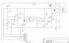
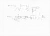
Late tonight I will try and upload some circuits I have made so you can see what I'm talking about.

Thanks,
Steve
 
Last edited:
A timing diagram would help us to understand what you want.

Based on a brief read (I'm time limited this morn - have a train to catch) of your post, I suspect you need an edge triggered device such as a monostable. A dual monostable would give you the initial delay from one mono and the following pulse from the second. Alternatively, an oscillator driving a counter may be suitable.
 
The input trigger to a 555 monostable must be shorter than its timed period or the timed period is extended. Use an input coupling capacitor and a resistor to the positive supply to shorten the trigger time then it will work fine when it gets a long duration input trigger.
 
Ok I made some timing diagrams, I had to use MS Paint because I dont have anything else to use here at work.

Fig1 - This is what is happening with my current OPAMP circuit, the output pulse is probably 1/4 of a second

Fig2 - This is the OPAMP circuit when it works (the power setpoint is below 3V)

Fig3 - This is what I would like the circuit to do when the power setpoint is higher than 3V

Fig4 - This is what I would like the circuit to do when the power setpoint is below 3V


I tried using 2, 555 monostable, one to create the intial pulse (edge-triggered from the 'plasma on' signal) and the second 555 (negative triggered) to output a delayed pulse after the intial pulse timed out. The problem I had was the 1st 555 kept retriggering because the 'plasma on' signal was staying high longer than the pulses i was making.

audioguru- I want to say I tried your idea, and it didnt work , but I will try it again tonight. Maybe my componant values were a little off?

In all of the things I read, they kept saying the 555 has to have a shorter trigger pulse than output pulse, maybe I should try using a flipflop? I will have to buy some since I dont have any, but thats fine.

Thanks for your help so far.
 

Attachments

  • Fig1.JPG
    Fig1.JPG
    31.2 KB · Views: 200
  • Fig2.JPG
    Fig2.JPG
    30.5 KB · Views: 194
  • Fig3.JPG
    Fig3.JPG
    30.6 KB · Views: 205
  • Fig4.JPG
    Fig4.JPG
    31.7 KB · Views: 191
Actually to make this easier to understand and since I have the rest of the circuit working great.... all I need to do, is figure out a circuit that when the "plasma on" signal goes high, a pulse for 0.5 seconds is created and after the pulse times out, the circuit will ignore any high "plasma on" signal until the "plasma on" signal goes low again.

Hopefully this might make it easier to understand.


Thanks,
Steve


edit.... Wow I'm really thinking about latching Flip Flops now, I could use the ones with the ENABLE input...hmmm
 
Last edited:
Attached is my old circuit, using OPAMPS and relays... I would not like to use relays in my newer versions of my circuit.

This is the pinout of the DB-9:
Pin
1 - Ground
2 - N/C
3 - Ground
4 - N/C
5 - +15VDC
6 - Circuit Output
7 - Plasma On Signal
8 - Power Setpoint Signal
9 - N/C
 
stizzswizz said:
Actually to make this easier to understand and since I have the rest of the circuit working great.... all I need to do, is figure out a circuit that when the "plasma on" signal goes high, a pulse for 0.5 seconds is created and after the pulse times out, the circuit will ignore any high "plasma on" signal until the "plasma on" signal goes low again.

Here is my suggestion.

The "plasma ON" signal trigger a 0.5 second edge triggered monstable, TTL/CMOS, not 555. The monostable outputs change states. After 0.5 second, it will time out and output changes state again. No more triggering occurs even the "plasma ON" signal remains high as the monostable is edge triggered.

A separate voltage comparator monitors the "Power Signal voltage" and outputs a HIGH if the signal is higher than 3V. This part works all the time.

Then fit a D type Flip-flop with the clock line(assuming positive edge triggered) triggered by the /Q of the monostable. The D input is always high. The reset pin of this D FlipFlop is connected to the output of the voltage comparator so any time when the "Power signal voltage" is higher than 3V, the D FlipFlop will be reset and its output will always be LOW.

You obtain your final control signal at the Q output of this flipflop.

Only when "Power signal level" is lower than 3V will the "1" on the D FlipFlop input be clocked to the F/F output to give you a high after "plasma ON" goes high for 0.5 second.
 
About monostables.... apparently I really don't know what they are... I know they can be built from a 555, but are you saying that a CMOS monostable multivibrator is the same thing? I picked up some D F/F's and some J-K F/F's.

Obviously since you said:

by the /Q of the monostable

its a F/F of some kind. I'll do more research tonight...

Thanks

edit.... I know what monostable means but am just asking about the different ways to make them.
 
Last edited:
stizzswizz said:
Attached is my old circuit, using OPAMPS and relays... I would not like to use relays in my newer versions of my circuit.

This is the pinout of the DB-9:
Pin
1 - Ground
2 - N/C
3 - Ground
4 - N/C
5 - +15VDC
6 - Circuit Output
7 - Plasma On Signal
8 - Power Setpoint Signal
9 - N/C


I just realized that I never attached the schematic, I'll post it tonight incase anybody wants to check it out.
 
The advantage of using a monostable over a 555 is that they are edge triggered and therefore don't need a RC differentiator circuit to generate a trigger pulse. All they need is a RC for timing.

My understanding of what you need is as follows:-
A mono triggered by the + edge of the Plasma on signal, a threshold detector to determine whether the Power set point voltage is >3V or <3V. The output of this goes to either the D input of a D type FF or to the J input of a JK FF (with K connected to 0)

The clock input (Ck) to the FF is triggered by the Q' (ie. Q bar) of the mono, or if you use a FF with a -ve edge trigger then Ck can be connected to Q.
 
Last edited:
Here is an inverting Schmitt Trigger (the "threshold detector" in my previous post).
I believe you need an inverting one since you want the output to be High if the Power Set Point voltage is < about 3 V.
I would therefore design the Schmitt for Vt+ of about 3 Volt and Vt- for say 2.7 Volt. This will give you 0.3 V of hystersis which should be adequate.

Edit, forgot to attach
 

Attachments

  • Schmitt Trigger.gif
    Schmitt Trigger.gif
    5 KB · Views: 161
Last edited:
ljcox said:
Here is an inverting Schmitt Trigger (the "threshold detector" in my previous post).
I believe you need an inverting one since you want the output to be High if the Power Set Point voltage is < about 3 V.
I would therefore design the Schmitt for Vt+ of about 3 Volt and Vt- for say 2.7 Volt. This will give you 0.3 V of hystersis which should be adequate.

Edit, forgot to attach


I like the idea of the Schmitt Trigger, I didn't think to use one in my application but I will use it in my new design.

Thanks
 
stizzswizz said:
I like the idea of the Schmitt Trigger, I didn't think to use one in my application but I will use it in my new design.

Thanks
Here is a suggestion. (Please excuse the scribble)

You don't need a Mono or a FF provided that the signals remain constant as you showed in your waveform diagrams 3 & 4.

Circuit description.
When PoS goes High, Cx charges via Rx. When the Cx voltage reaches the +ve threshold of IC1a, X goes High.

In case 1, I have assumed that the PSP voltage rises to +6 Volt.
Thus the output of the Inverting Schmitt Trigger remains Low.
Hence the output remains Low.

In case 2, I have assumed that the PSP voltage rises to +2 Volt.
Thus the output of the Inverting Schmitt Trigger goes High.
Hence the output goes High.

When PoS goes Low, Cx discharges rapidly via D & Rr thus the circuit is reset ready for the next sequence.
 

Attachments

  • Plasma Circuit.gif
    Plasma Circuit.gif
    28.4 KB · Views: 158
Ok... So this is my delay correct?

When PoS goes High, Cx charges via Rx. When the Cx voltage reaches the +ve threshold of IC1a, X goes High.

I actually have a similar sketch I made, using a standard voltage comparator and NAND gates. All I had to add to the circuit were RC timing componants, but I didnt know my threshold voltage for the NAND gate.


Also couldnt I use a standard voltage comparator instead of a Schmitt Trigger? The signals the circuit will be getting are straight from a PLC.

I'm stuck at work for another hour! I can't wait till I get home to start to really crank out a couple ideas on OrCad!
 
stizzswizz said:
Ok... So this is my delay correct?

I actually have a similar sketch I made, using a standard voltage comparator and NAND gates. All I had to add to the circuit were RC timing componants, but I didnt know my threshold voltage for the NAND gate.

Also couldnt I use a standard voltage comparator instead of a Schmitt Trigger? The signals the circuit will be getting are straight from a PLC.
Answers
1. Yes. The delay is the time to charge Cx to the +ve threshold level of the IC1a Schmitt NAND.

2. A standard voltage comparitor (or an Op Amp configured as a comparitor) does not have hystersis. Whereas, a Schmitt Trigger is a voltage comparitor with positive feedback so that, once the voltage reaches the threshold, it changes rapidly.

Question - what is a PLC?
 
Question - what is a PLC?

A PLC is a Programable Logic Controller. Its bascially a PIC with its inputs and outputs isolated and boosted with transistors. On the PECVD tool I use there are two PLCs connected to a computer and they allow me to control the tool and monitor all the connected sensors via software.

Now the easy thing to do would be to program the PLC to output a signal when the power setpoint is below 3V, but we can't get the software to program the PLC and we don't feel like paying at least $5k to have it reprogramed on-site from the vendor.


About hystersis, I was always under the impression that hystersis was a bad thing. I thought a standard voltage comparator had hystersis (when both inputs are close to each other and it toggles the output rapidly). By adding a type of feedback to one of the inputs it would take care of that, it will reduce your "hystersis level".

I'll mess around with the componants I have and refresh my mind about Flip Flops, I'll let you know when I have a schematic drawn.

Thanks
 
stizzswizz said:
Attached is my old circuit, using OPAMPS and relays... I would not like to use relays in my newer versions of my circuit.

This is the pinout of the DB-9:
Pin
1 - Ground
2 - N/C
3 - Ground
4 - N/C
5 - +15VDC
6 - Circuit Output
7 - Plasma On Signal
8 - Power Setpoint Signal
9 - N/C


Schematic Attached
 

Attachments

  • Old version1.JPG
    Old version1.JPG
    91.2 KB · Views: 143
Here's the idea I had using an RC circuit connected directly to the NAND gate.
 

Attachments

  • NAND Threshold Timer.jpg
    NAND Threshold Timer.jpg
    104 KB · Views: 153
About hystersis, I was always under the impression that hystersis was a bad thing. I thought a standard voltage comparator had hystersis (when both inputs are close to each other and it toggles the output rapidly). By adding a type of feedback to one of the inputs it would take care of that, it will reduce your "hystersis leve

I did some research and found out that I was thinking completely opposite. :eek:
 
When detecting threshold levels, hystersis good not bad. Without hystersis, the trigger level is not precisly defined and the transitions are slow.

Hystersis is particularily important for an RC timer because an Op Amp or Voltage Comparitor is a high gain amplifier so without hystersis, the output will change slowly as the input voltage passes through the linear range.

So in the circuit you posted, you should replace the 4011 with a 4093.

Also, you don't need the opto coupler and 555.
 
Status
Not open for further replies.

Latest threads

New Articles From Microcontroller Tips

Back
Top