Continue to Site

Welcome to our site!

Electro Tech is an online community (with over 170,000 members) who enjoy talking about and building electronic circuits, projects and gadgets. To participate you need to register. Registration is free. Click here to register now.

  • Welcome to our site! Electro Tech is an online community (with over 170,000 members) who enjoy talking about and building electronic circuits, projects and gadgets. To participate you need to register. Registration is free. Click here to register now.

OFF-the-wall idea for momentary ON switch

MrDEB

Well-Known Member
Looking to build a digital kitchen timer that shuts off after timing out and/or a 10 second delay waiting for user input.
Here is the screenshot of the on/off section of the kitchen timer. Going to use an 18Fxxxx pic
maybe need a diode on the pic output pin to prevent applying voltage to the unpowered pic.
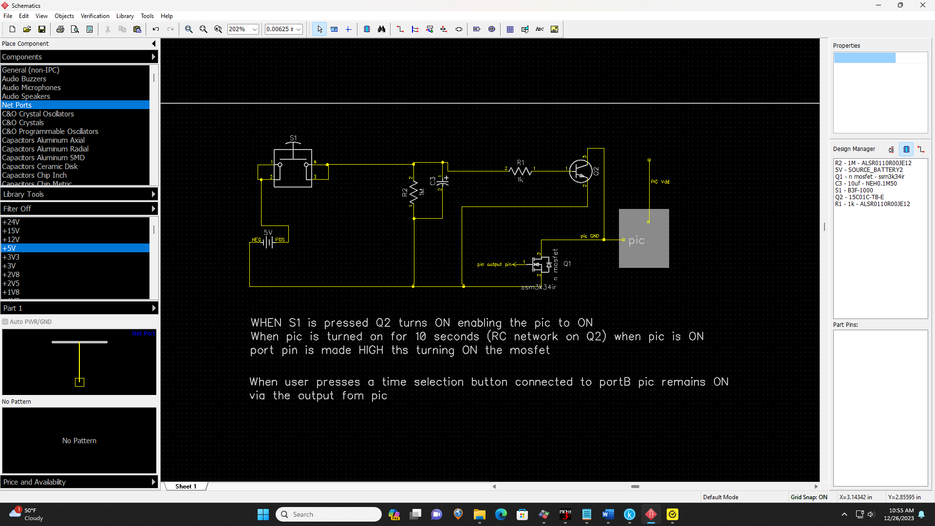
Screenshot (38).png
unpowered pic?
 
Since you haven't acknowledged my comments regarding the LCD and its backlight never turning off nor my comments about separating GND from "ground", I figured I should explain this in detail because it's a critical point.

Your circuit is switching the GND connection to control power to the micro. You want to make the same connections for the LCD and its backlight and everything else that should only be on when the micro is on. The GND symbols you have scattered about defeat this purpose.

In your marked up schematic shown below (maybe you've already straightened this out but you haven't posted an updated schematic so I don't know) the GND symbols shown in red circles are actually ground. The GND symbols shown in brown circles ARE NOT ground - they are the switched "ground" connection from the mosfet. Using the GND symbol for these connections will lead to all of these points connected to GND, defeating your timer circuit.

You do have a major complication with the ICSP connection. Your PICkit 3 may not provide enough power to power the micro, LCD and its backlight. If it can, you'll want to connect it to the "brown circle ground" so that timer circuit won't interfere during programming. If the PICkit 3 won't supply enough current (where is +5V coming from?), then the ICSP ground should be connected to "red circle" true ground. In this case, I guess the easiest option is to have a 2-pin header across the mosfet to bypass the delay circle during dev.

Note: my comments apply only to the marked items on this schematic discussed above. There may be other errors I haven't mentioned.

mrdeb ground.png
 
The red line across the cap under the micro means remove the cap and connect those points.
 
Be sure you separate grounds and think about the ICSP issues.
 
I have programmed a pic w/lcd but turn on the battery.
here is a revised schematic that I made several changes to using the links from post#23
schematic_4.jpg
 
You still don't show the control lines to the LCD.

The difficulty about using ICSP to program with the switch circuit still applies.
 
But switching V+ definitely is better in my opinion.
 
I don't follow that schematic. When the start switch is pressed, the collector of Q2 goes to 5V, the PIC can then turn on Q2 and ground the Collector!

Mike.
Edit, the more I look at that schematic the more problems I see.
 
here is a revised schematic that I realized while writing a description I had the previous schematic wrong (changed the collector to make Q1 gate LOW

Pressing START turnson Q4 which turn on Q1 mosfet


the +5V then turnson the micro and enabling the RC network (c4/R7) allowing a 10 seconddelay


the micro is enabledwhen it receives power (+5V)


portA.3 turns on Q2which takes the gate of Q1 low thus keeping the micro ON.
schematic_5.jpg
 
The latch circuit in MrDEB 's latest schematic is from Electonoobs and is somewhat clearer in my latch circuits collection in post #12. I must admit I missed a connection in that schematic - here is the corrected version (I'll correct the versions in post #12 shortly). The operation is explained in the link above.

corrected latch circuit.png
 
Just out of curiosity Mr DEB, how will you read those (on the left) swiches? The input pins will be 5V or floating. You could turn on the internal pullups and then they'll read high all the time. Or, does that particular chip have internal pull downs?

Mike.
 
how will you read those (on the left) swiches?
Good point!

Also, /MCLR must be pulled high. As it's drawn, the resistor is connected to }+5 on the ICSP connector, but it's not connected to +5 of the circuit.

1704322778217.png
 
here is a revised schematic that I realized while writing a description I had the previous schematic wrong (changed the collector to make Q1 gate LOW

NO. Please don't change connections of circuits you don't understand. The operation is explained quite nicely on Electronoobs page. SMH
 
Good point!

Also, /MCLR must be pulled high. As it's drawn, the resistor is connected to }+5 on the ICSP connector, but it's not connected to +5 of the circuit.

View attachment 143953
Also, the Pickits look for Vdd or decide it's connected wrong. Or the Pickits must be set to power the circuit, which should work.

Mike.
Edit, as long as the external 5V supply is maintained.
 
Another excellent point. I was thinking that it was probably best to leave V+ disconnected because the PICkit 3 can't supply much current. But you are correct – it must be connected for the PICkit to work.

A jumper to bypass the cutoff circuit during dev would be a good idea.
 
A jumper to bypass the cutoff circuit during dev would be a good idea.
+1

For the circuit in #51, couldn't you leave out C2?

The only "disadvantage" I see is that you'd have to have the button depressed until the uC ran and turned on Q4, but that's pretty quick, maybe 10's of msecs.
 
If you want something simpler, why not just use a high-side load switch like the TI TPS2061DBV?
That would handle about 1A-1.5A and gives you current-limiting protection too.

It has a low-active enable input /EN, so connect /EN to IN via a 10K resistor, and then connect both the PB switch and PIC IO pin to /EN. The PB would connect /EN to GND to turn it on, after which the uC would set its IO pin low to keep /EN on. To turn off the uC could just set the IO pin to input mode.

Single SOT23 package, cost ~ $1. Comes in a variety of packages with status output, duals, etc.
 
Don't most regulators have an enable pin that could be used in the same way?

Mike.
I don't know about 'most', but some certainly do - however, the enable pin doesn't entirely turn the regulator OFF, it switches the output OFF, but it usually still draws current from the supply (I looked in to various such regulators). Hence the circuit I posted above, which draws zero current when switch OFF.

Incidentally, the MicroChip 250mA regulator MCP1702-3302E is a small 3.3V 3 pin through hole regulator, is LDO, and has a VERY low quiescent current, I use them for powering PIC's that are in sleep to minimise current draw. Much better than the 78Lxx regulators, but you need to be aware the pinouts are completely different.
 

Latest threads

New Articles From Microcontroller Tips

Back
Top