Electro Tech is an online community (with over 170,000 members) who enjoy talking about and building electronic circuits, projects and gadgets. To participate you need to register. Registration is free. Click here to register now.
Welcome to our site! Electro Tech is an online community (with over 170,000 members) who enjoy talking about and building electronic circuits, projects and gadgets. To participate you need to register. Registration is free. Click here to register now.
Generally, strips are 12-v rails with "bus bars" down each side and at 1-inch or 2-inch intervals there are a series of three LEDs and a resistor to limit current. Some newer strips have 4 high efficiency per series with one resistor.
As long as the pulldown is connected BEFORE the series R then it's not a voltage divider... you'll get the full voltage swing on the gate. If the series R is connected first then you have a voltage divider, which you probably don't want since it'll reduce the gate drive voltage.
The series R will interact with the gate capacitance, slow down the turn on/turn off time, and very likely increase the power consumption of the mosfet. It'll do this no matter if you have the series R connected before or after the pulldown.
Slowing down the edges isn't necessarily a bad thing... it'll help reduce any switching transients, but it will likely make the mosfets run hotter depending on how often you switch them.
The pulldowns are really there so that the mosfets don't all turn on when the board is powered up/down, before the drive signals are initialized.
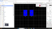
I laid out a footprint with 18mm wide heatsink areas, which should just all for 8 MOSFETs on a 150mm wide board. It was just easier than trying to explain the process. 18mm wide doesn't provide a lot of heatsink area, but it's a starting point you can edit.
Referring to post #63 I think the measurement is incorrect.
Looking at the datta sheet I come up with different figures.
Using the high-end and low end measurements
15.24 - 2.61 = 12.63 add 4.06 = 16.67
14.84 - 2.62 = 12.22 add 3.55 = 15.77
round it out and I come up with 16.666
not saying popcore is wrong, just questioning?
If the distance between mounting hole and the bend point of the leads (where they narrow down) is too large, just bend the leads a little farther down. If the distance is too short, then you'll need to bend the leads in the wide area, which has the potential of damaging the bonds inside the case.
You're probably fine with the shorter distance, which is about what I had initially, but on a different drawing, it looked tight, so I extended the distance a bit.
I imported the first one you posted but it had no bottom layer.
I copy n pasted the second one with via stitching. All was good then bam! The stitching disappeared. I think Easyeda has several bugs. The program froze up yesterday as well. Going to recover the file and hopefully get a pcboard.
Plan to have the board assembled as the mosfets are 4x less than what I paid for from Mouser etc.
Copy and pasted? From where? To where? You didn't "open EasyEDA file"? Will I never learn?
You do understand that if JLC assembles the boards, it will be 10 copies? And that you'll need to explain every detail fully? Like how you expect the MOSFETs to be mounted?
In my experience, EasyEDA iscl very solid. If it's acting goofy, save your file, go to task manager and close EasyEDA, then restart it. Perhaps rebooting the computer isvl a goodvl idea too.
I downloaded the file you posted and then copied and pasted the mosfets.
I get a top and bottom layer.
I need to recheck JLC bt recall seeing where only 2 boards are required for assembly.
can't find the page that showed only 2 boards required.
Sent a message to Diptrace about increasing the number of connections. Have gotten an upgrade in the past for more than 300 connections.
Easyeda is a nice program but it has bugs. I have a board but the DRC says I have issues. Very confusing at best.
Sorry, my footprint does not work properly. There's no apparent way to associate the vias and plane areas to the same net. The quick and dirty approach won't work.
This site uses cookies to help personalise content, tailor your experience and to keep you logged in if you register.
By continuing to use this site, you are consenting to our use of cookies.