Continue to Site

Welcome to our site!

Electro Tech is an online community (with over 170,000 members) who enjoy talking about and building electronic circuits, projects and gadgets. To participate you need to register. Registration is free. Click here to register now.

  • Welcome to our site! Electro Tech is an online community (with over 170,000 members) who enjoy talking about and building electronic circuits, projects and gadgets. To participate you need to register. Registration is free. Click here to register now.

Making a pcb

Status
Not open for further replies.

peter g

Member
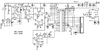
hi all, i want to make a pcb. the pcb has the standard black on a white backround. also included is the parts placement which is outlined in red. my question is will the red lines effect the pcb making process? will the red still be there after i etch or will the red not affect the etching process? i hope i'am presenting this correctly.
 
What software are you using to generate the Gerber file? Also usually the parts placement outlines do remain on the board (how would you know where to put the components otherwise), but it usually remains as a black or white outline. If you have the Gerber file, I could take a look for you.
 
hi, i don't have a gerber file, this project is 10 years old. most of the time the parts placement is a separate diagram and not superimposed on the pcb. i don't understand how you can make the board withe red lines interfering?
 
No one here knows what your talking about, apparently.

In the "old days", PCB layouts were taped with red, black and blue tape. Black was on all layers. For red and blue, I forget which was which. Black could be imaged with blue and color separated. Same for red.

The silk screen was yet another layer. So, you had maybe 4 sheets of mylar layed out at maybe 4x.

That's not done anymore.

I gather you have a single sided board with a red silk screen.

You should be able to separate with photoshop. e.g. change red to the transparent color or whatever.

Another alternative is to use PCB making software that gives you some help to reverse engineer it or if you have the schematic, do it correctly.

one such piece of software is Target 3001.

the cost of having PCB's made is so small it generally doesn't make sense to do it yourself.

The files you submit are known as Gerber files, one for each layer; then there is the board outline and a drill file.

These you send in a ZIP file by email and shortly your boards show up say shipped by DHL.
 
I'm guessing it is a PCB image in a magazine article or something like that?

And the OP wants to make a board by toner transfer or photographically, from the printed layout.
edit - typo.
 
Last edited:
yes, toner transfer. when i print the pcb image, the red outline of the parts placement which is also outlined on the target pcb also gets printed. when i apply the toner image to the blank pcb the lines for the parts placement also get printed which causes shorts, etc. which means when i etch the board, the outline of the parts placement also is etched causing shorts,etc. the suggestion about using paint is a good one, but i've tried that to no avail. can anyone guide me thru the process of getting rid of the unwanted lines using gimp/paint? is this clearer?
 
this is the file.
 

Attachments

  • cesr meter pcb.png
    cesr meter pcb.png
    45.4 KB · Views: 206
OK; unfortunately the red is overlaid on the black, there is no colour difference in it whether over black or white.

The only way to do it is manually erase all the red and replace with black where it was over PCB traces...
 
WOW! jrw, you the man! thanks so much, now i can proceed with the build. btw, if anyone is interested google LCM3 esr meter, i've built it and it works great. again, thanks to ron and jrw. thanks ron for the pictures. happy!
 
Status
Not open for further replies.

Latest threads

New Articles From Microcontroller Tips

Back
Top