I am trying to create a simple half bridge inverter in LTSpice. I have chosen to use a purely inductive load and I am having some problems with the circuit.
I am using a gate driver the IR2110a to drive the MOSFETS.
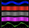
The problems I am having are the output voltage (Vs-Va) is not as expected. I was expecting the midpoint between the capacitors C3 and C1 (Va) to be constant at a value of Vrail/2 but it is oscillating as a sine wave which I believe may be causing this issue. Why is Va acting in this way?
Another issue (which may be linked) is the value of Vs becomes greater than Vrail at times in the circuit- due to the inductive load- is this normal or can I solve this? Am I correct that the high side mosfet cannot function correctly if Vs becomes higher than Vrail while M1 is on and the current will flow through D2 causing M1 to be ineffective?
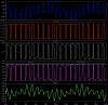
Below is the LTSpice circuit and the output graphs, I have done it here at 100Hz pwm frequency and 1kHz and 10kHz pulse frequency
I have tried changing a number of parameters such as capacitor values, rail voltage and frequency to solve the issues with no success.
If anyone has any explanations or solutions of what I am doing incorrectly that would be much appreciated.
Any queries about the circuit or what I am asking let me know

I am using a gate driver the IR2110a to drive the MOSFETS.
The problems I am having are the output voltage (Vs-Va) is not as expected. I was expecting the midpoint between the capacitors C3 and C1 (Va) to be constant at a value of Vrail/2 but it is oscillating as a sine wave which I believe may be causing this issue. Why is Va acting in this way?
Another issue (which may be linked) is the value of Vs becomes greater than Vrail at times in the circuit- due to the inductive load- is this normal or can I solve this? Am I correct that the high side mosfet cannot function correctly if Vs becomes higher than Vrail while M1 is on and the current will flow through D2 causing M1 to be ineffective?
Below is the LTSpice circuit and the output graphs, I have done it here at 100Hz pwm frequency and 1kHz and 10kHz pulse frequency
I have tried changing a number of parameters such as capacitor values, rail voltage and frequency to solve the issues with no success.
If anyone has any explanations or solutions of what I am doing incorrectly that would be much appreciated.
Any queries about the circuit or what I am asking let me know