Continue to Site

Welcome to our site!

Electro Tech is an online community (with over 170,000 members) who enjoy talking about and building electronic circuits, projects and gadgets. To participate you need to register. Registration is free. Click here to register now.

  • Welcome to our site! Electro Tech is an online community (with over 170,000 members) who enjoy talking about and building electronic circuits, projects and gadgets. To participate you need to register. Registration is free. Click here to register now.

Level translation

Status
Not open for further replies.

jayce3390

New Member
Hello,

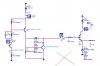
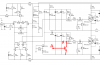
From the output of a low side driver (0V / 5V) I need to make a level translation to get (0V / 65V) at the input of a N type MOSFET.

I tried with the following circuit using general purpose npn et pnp devices from motorola, it's really slow but it works. (see included file )

This circuit must be as fast as possible, with minimum number of components. Could you give me an idea to do a faster circuit?

thank you
 

Attachments

  • level shifter circuit.jpg
    level shifter circuit.jpg
    104.5 KB · Views: 555
Last edited:
that is a typical gate driver and practically the fastest.

if you really want, you may look into dedicated driver ICs.
 
...This circuit must be as fast as possible, with minimum number of components. Could you give me an idea to do a faster circuit?

What is the value of R4? R4 and the gate capacitance of the FET could well be the dominant slew-rate limiter.
 
R4 value is 10 ohms.

millwood, I use a fast low side gate driver (el7457) before this circuit level translation.
The level translation makes the global circuit slower.

If I use NMOS end PMOS in totem topology? what do you think about that?
 
Last edited:
10ohm is about the high-end of the range.

is it turn on too slow or turning off too slow? this should be good for a few hundred khz.

if it is much faster than that, it may require more work.

take a look at the attached schematic. it is from a Philips application note on their Class D amp running at 400khz. the two mosfets are driven by two discrete gate driver. the low side consists of Q7, Q9 and Q11. When Q7 turns on, it turns on Q9 which charges up the gate. When Q7 turns off, it turns on Q11 and drains the gate charges.

I penciled in a red npn in place of Q7 as your signal input.

if you go n-channel and p-channel, you for sure w ill need a gate driver of high current output to overcome the gate capacitance - so it may not be more advantageous to you.

I would stay with a discrete or with some dedicated (low-side) gate drivers. try microchip or TI for some.
 

Attachments

  • level shifter.PNG
    level shifter.PNG
    53.2 KB · Views: 1,284
Mosfets will be faster than bjts for drivers, but it's hard to find very low Cgs mosfets. I'm working on this very problem right now, playing with different configurations in LTSpice.

It really sucks, because the comparators I'm using will only source 11ma. LTSpice doesn't seem to have any logic level mosfets either, or I just can't tell them apart from the normal ones.
 
Last edited:
Finally, I forgot to set up the proper step time in my transient simulation, the step time was too large, leading in wrong result.

It seems it's quite fast. Do you know if the P/Ns I m using (bipolar transistor) are a good choice?

Remind :
PN2907
2N3904
Vcc (required) = 70V

Millwood, the picture you show looks like my circuit, but with different BJTs, can I use the same ones in my application?
 
2907 is rated 60v and 3904 40v.

and depending on the load / circuit configuration, you may want to double that when you are dealing with inductive load.

so I would get parts rated 130v or more. and my favorite there is 2n5551/2n5401 (150v parts).
 
Thank you, I will try these P/Ns.
I m trying to find BJTs able to follow the low side driver output which is very powerful at high frequency.
the driver can manage more than 40 MHz of input signal frequency.

The load is composed of a mosfet with a gate resistor, I think it's more capacitive/resistive than inductive.
 
the upper mosfet's source is tied to the switching node, which could be tied to an inductive load (aka an inductor in a class D amp). so some of the bjts in the upside driver can be swung below the ground.

40mhz is extremely high and I am not sure if you can find any output devices at that kind of frequencies, and 2n5551/5401 certainly wouldn't work at that kind of frequencies: they are good at about 1mhz and if you don't care much about signal integrity, they can be used at up to 10mhz but anything above that is going to be probamatic.
 
Yes in the picture you showed, I m using only one mosfet in a basic buck converter, the only inductance I have is located inside my buck converter, it could be a problem, indeed.

Yes, If I can do 5 or 10MHz I will be happy.

I see the 2n5551, the Ft is between 100-300 MHz, it's quite good.
 
in that case, the "kick-back" diode will be a shottkey diode and you don't need to worry about 2x supply voltage.

it will be very difficult to make it run at anything north of 1mhz - you will have lots of difficulties finding a mosfet capable of running at that level, and it will be even harder on layout and to contain emf interference.

I have used 5401/5551 for a long time because they are dirt cheap - I buy them in hundreds and they are pennies each.
 
Yes, actually you are right, the mosfet used in the buck will also restrict the global speed capability.
I use an 7380 from IRF.
I really don't have background on BJTs, that's why I appreciate any information.

Why did you note that the "kick back' diode should be a shottky? I don't understand that.
 
Last edited:
the way a buck converter works is by "kicking back" the current when the switcher shuts off. that Schottky diode provides the path for the inductor to maintain the current flow in the circuit.

it provides the same function as a "kick back" diode you put on a relay.
 
Freewheel diode might be a better name. Kick-back is a bit of a misnomer as it doesn't reverse current flow or voltage, it just needs a path to keep flowing in the same direction. Since the switch is open when the inductor "discharges", it can't use the usual ground for the energy loop. The diode completes a different loop where the current can flow.

When the inductor first starts discharging, the voltage ramps up until it is higher than the switching node voltage plus the diode forward drop. Then it ramps down as it has a path to flow, until it falls below the diode voltage. It then starts ramping up again until it cross the threshold. This "ringing" happens very quickly, which is why a schotkey or "fast recovery diode" is used. It needs to be able to turn off very quickly to prevent leakage from the switching node to ground.

Hope that explained the diode question. :)
 
10ohm is about the high-end of the range.

is it turn on too slow or turning off too slow? this should be good for a few hundred khz.

if it is much faster than that, it may require more work.

take a look at the attached schematic. it is from a Philips application note on their Class D amp running at 400khz. the two mosfets are driven by two discrete gate driver. the low side consists of Q7, Q9 and Q11. When Q7 turns on, it turns on Q9 which charges up the gate. When Q7 turns off, it turns on Q11 and drains the gate charges.

I penciled in a red npn in place of Q7 as your signal input.

if you go n-channel and p-channel, you for sure w ill need a gate driver of high current output to overcome the gate capacitance - so it may not be more advantageous to you.

I would stay with a discrete or with some dedicated (low-side) gate drivers. try microchip or TI for some.
Your red NPN needs current limiting resistors in series with the collector and the base.
 
It seems that I don't have to connect the collector of BJT PNP Q6 to the MOSFET source, in contrast with the picture that you post Millwood.
(See attached picture)

If I tie, the circuit doesn't work. Why? Do you have an idea?
 

Attachments

  • Sans titre.jpg
    Sans titre.jpg
    27.8 KB · Views: 156
Status
Not open for further replies.

Latest threads

New Articles From Microcontroller Tips

Back
Top