Continue to Site

Welcome to our site!

Electro Tech is an online community (with over 170,000 members) who enjoy talking about and building electronic circuits, projects and gadgets. To participate you need to register. Registration is free. Click here to register now.

  • Welcome to our site! Electro Tech is an online community (with over 170,000 members) who enjoy talking about and building electronic circuits, projects and gadgets. To participate you need to register. Registration is free. Click here to register now.

Level translation

Status
Not open for further replies.
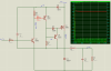
I am not sure why it is not working. here is a quick simulation I put together.

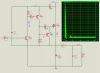
the source is a 20k square wave (3.3v), and typical values. the output is a 15vdc into a 10ohm load, through a 33uh inductor and a 47u cap.

it seems to work just fine, in simulation at least.
 

Attachments

  • hs driver.PNG
    hs driver.PNG
    47.7 KB · Views: 126
The value of resistor R3 between collector and base of PNP is 1kΩ in my case.

If I reduce this value to 0.1kΩ, the circuit works with collector of Q6 connected to the mosfet source .

If not, it doesn't work.
 
The value of resistor R3 between collector and base of PNP is 1kΩ in my case.

If I reduce this value to 0.1kΩ, the circuit works with collector of Q6 connected to the mosfet source .

If not, it doesn't work.

I think you are talking about R4 in my schematic.

here is a sim for R4=.1k. it appears to work just fine.

when you say it doesn't work, what does it do?
 

Attachments

  • hs driver 2.PNG
    hs driver 2.PNG
    45.8 KB · Views: 109
When I said it doesn't work , I meant that the voltage at the MOSFET gate was not switching. I obtained a constant voltage around 60-70V, that put the MOSFET in "ON" mode everytime.


I was talking about R4 in my schematic, but this is also R4 in yours.
At the beginning the value I put was 1kΩ.

I reduced to 0.1kΩ with Q6 collector tied to the MOSFET source and I obtain the result in the picture attached, at the output of the buck converter with an input signal at 4 MHz.

The duty cycle is varying from 50% to 25%. What do you think of that?
 

Attachments

  • graph.jpg
    graph.jpg
    19.8 KB · Views: 119
4mhz is the difference - i was running my sim at 20khz. at 4mhz, 1k resistor at R4 may not be enough to charge up (current being too small) or to bleed the gate capacitance - but that's why you have Q4 there.

well, if .1k works, stay with it.

as to the duty cycle, whether it is sufficient depends on your supply voltage, load, and load dynamics, to name a few.

the charts are very small to see. Are they traces of output voltage? it should be much better than that, unless you are driving a dynamic load. the output voltage should be rock solid on a static load (+ static input voltage).

here is what I have running at 200khz. the red trace is the output voltage.
 

Attachments

  • hs driver 3.PNG
    hs driver 3.PNG
    47.6 KB · Views: 107
Ok thank you, I didn't realize it.
These traces are at the load (50Ω) of the buck converter as you can see in the picture attached.
the load is a static load, but for the ripple, I was simulating with a time stop of 200 us, in contrast with you 2 ms.

Maybe if I extend it, it will be flat.

Please,could you show me the voltage waveform you have at a node located at the mosfet gate?
 

Attachments

  • buck.jpg
    buck.jpg
    118.8 KB · Views: 99
Last edited:
Please,could you show me the voltage waveform you have at a node located at the mosfet gate?

here it is.

Vg is the voltage on the gate (vs. ground). Q1's gate.

Vsw is the voltage on the switching node (vs. ground). Q1's source.

so Vgs = Vg-Vsw

Vin is the input signal (vs. ground), 3.3v pulse at 20khz.
 

Attachments

  • hs driver 4.PNG
    hs driver 4.PNG
    66.5 KB · Views: 117
all the voltage traces are for the right vertical axle.

the green trace is the power dissipation on the mosfet, for the left axle. looks like it averages about 15w.
 
thank you very much. Look at my waveforms, it is almost comparable, the simulation is performed at 1 MHz, and the duty cycle is varying.


Vin is a square waveform at 1 MHz from the driver.

Vg is the voltage at the MOSFET gate.

It seems Vg period is twice Vin period, maybe it's due to the BJTs stage, which is quite slow at 1MHz.
 

Attachments

  • waveforms.jpg
    waveforms.jpg
    104.4 KB · Views: 108
without a plot of Vs, it is tough to tell.

However, if you look at my waveform, when the Vin is 0, the Vg goes to zero (slightly negative) to bleed the gate capacitance, and then it bounces back at about 15v - the output voltage. so the mosfet is fully shut off and remains off during that part of the cycle.

in your waveform, when Vin goes 0, Vg starts to decline, and continues to decline, but slowly, to zero. without knowing where Vs is, it is not clear if the mosfet is eventually shut off but it is sure that its shut off is gradual. This means high Pd turning of the mosfet off - not something you want.
 
Ok
In my case the voltage drop at the mosfet gate is too slow, and then the mosfet is not fully off.
But how to explain the obtained waveforms at the buck converter output?

According to the Vgate waveform, the buck converter should not work, isn't it?
I attached a picture of the waveforms obtained with a 2 MHz input signal, the duty cycle moves from 50% to 25%.

Vg : voltage at the mosfet gate
Vs : voltage at the mosfet source
Vload, Iload : at the buck converter load
Vin : signal at the driver output
 

Attachments

  • waveforms.jpg
    waveforms.jpg
    59 KB · Views: 107
The mosfet is still somewhat turning on and off, just not fully. There would be LOTS of power dissipation due to this though, as the mosfets are running in their ohmic region. The closer to a perfect PWM signal you can make it, the less switching and conduction losses you will have. Take the series resistor off the mosfet gate. It's not needed and slowing your switching down.

2Mhz is quite high. 1Mhz is the highest I've seen for switching supplies and that's for super tiny ones that only handle a few hundred mA. Why are you trying to switch so fast?
 
Last edited:
I removed the gate resistor, but the delay time is introduced mainly by my intermediate stage, which has 1us response time, really slow!!

I will have a lot of dissipated power as you said, nevertheless, this circuit could work?I mean, even if the MOSFET is not fully on/off.

thanks
 
Because, I need very high level of efficiency, >80%. You don't have RF amp working at such level. The power I need is around 130W.

From your other thread.

So if it's not an RF amp then why do you need such high frequency?
 
I will have a lot of dissipated power as you said, nevertheless, this circuit could work?I mean, even if the MOSFET is not fully on/off.

You will have to model the power dissipation to find out if the mosfets can handle that much power. But theoretically it could work.
 
I will try to explain with more details.
The circuit presented in this post is a kind of DC/DC converter, composed af a buck converter, his driver and a PWM, it looks like a power supply, isn't it?


But, the input signal at the PWM input is a low frequency signal, let say 5 MHz, this low frequency signal is actually the envelope of a RF signal which is used in an RF amp, the envelope signal is detected using an envelope detector.

This DC/DC converter will provide the dynamic voltage supply according to the time varying envelope to the RF amp, it's a way to improve the efficiency.
If you want the RF amp is the load of the buck converter.
 
You could get it faster by using mosfets for your drivers instead of BJTs. They switch to full on and off states much faster than BJTs do (orders of magnitude faster), and would cleanup the PWM signal going to the power mosfet.

I don't fully understand why yet, but it has something to do with there being no delays due to storage and recombination of the minority carrier. Plus, BJTs require a much larger reverse current to turn off as quickly.

5Mhz is a very lofty goal.
 
Last edited:
Thank you for your help guys.

Smanches you are thinking about a "totem-pole" (only 2 MOSFETs) topology with MOSFETs or I can directly replace all BJTs by MOSFETs?

I simulated the time delay introduced by the level shifting stage, the result is 1 us!!!
 
Status
Not open for further replies.

Latest threads

New Articles From Microcontroller Tips

Back
Top