Continue to Site

Welcome to our site!

Electro Tech is an online community (with over 170,000 members) who enjoy talking about and building electronic circuits, projects and gadgets. To participate you need to register. Registration is free. Click here to register now.

  • Welcome to our site! Electro Tech is an online community (with over 170,000 members) who enjoy talking about and building electronic circuits, projects and gadgets. To participate you need to register. Registration is free. Click here to register now.

Lets take a look on a linear amplifier

Status
Not open for further replies.
Hi there,

Hope my post find you well.
I would like to get attention some knowledgeble person in this post !

So, kindly avoid this post if you wont have experience.

I need to know this application well, because I want to develope a 3-phase-calibrator.
My application needs to amplify signal to a certain level.

Here we go ....
Explain kindly
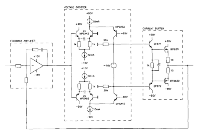
linear_amp.PNG


1. Its a Claas AB amp circuit.
2. Looks 200W capacity.
3. Explain its voltage booster.
4. Why current buffer is used?
5. Why should we care about " crossover distrotion"


Beside this circuit, I have a practical design.
I want to move class AB to Class D.

Thanks a lot!
 
Last edited:
You show a class-AB linear amplifier circuit that wastes a lot of power making heat. A class-D amplifier is completely different.
You do not say the frequencies you need or the load impedance.
 
Dear Sir Audio guru,
Its my pleasure to get you here again, praying for your long life and good health.

Yes, people said "its not Class D, it might be Class AB. Its may be 200W.
Nothing Class D about it, but you can of course feed it with a square wave signal if you like.

Power stage quiescent current is set with the "~10 V" voltage in the middle (which should be thermally coupled/compensated with the output MOSFETs)p.

Lets post a basic image here
01xJr.png


May be 13 years ago I have atudied this circuit.
In this style, NPN and PNP transistor has connected back to back. Vcc is used at the top, while other collector is grounded.
Like audio power amplifier, output is not taking from collector, its from combined emmiter.
Input and output capacitors are DC bloking capacitors? What load will see then!

Biasing resistance and diodes are maintaning input voltage. One cycle signal has been shared both of transiator's base, not sure forward and reversed biased diodes are helping to conduction, may be 1N4148 type.

Now interesting to see how the signal is amplified, for sure its not phase shift! Depending on amplification factor, it will talk. I think bandwidth is too narrow. For the high frequency application, we need to think.

My current design might be class AB type.
Its feedback opamp is 551, input series RC element is 13k, 1uF.

Feedback parallel element may be 4.7 k, .33uF. Output has .33u and 10ohm series RC.

I am using TIP147, TIP142, C1815, A1015. They are properly biasd like cascaed 3 stage, may be AB class network. More symmetric way, like one pairs AB class output is connected to others pair. Last pairs base is connected to first pairs base! At last a voltage divider of 5 ohm has been made between 2nd and 3rd outputs!


Biasing voltage of this amplifier is plus, minus 24 volt.
The problem I am facing is heating !
Lets disscuss more for a Class D to have a solution.
 
In a conventional audio amplifier, a lot of the design effort relates to maintaining linearity and avoiding crossover distortion.

In a Class D amp, that is all totally irrelevant - it's a pulse-width modulator and power switch and the idea is purely to minimise switching losses, so the output is as close as possible to the + or - supply, depending which way it is switched.

"Audio" only exists up to the input of the modulator and after the output filter - not in the power electronics stage.


A half-bridge PWM motor driver is the close to the same power structure; anything relating to conventional audio amps is out the window when you change to digital modes.


The second post in this thread shows a power stage that is in principle suitable for a class D amp:

Or one side of an H bridge circuit such as this, adapted for whatever supply voltage is needed:

The essence is that the power circuits are designed for fast and efficient switching, not in any way for linearity.


The PWM carrier frequency must also be high enough that it is easy to filter out without undue attenuation of the highest audio frequency the amp is required to function with.
 
Dear Sir rjenkingb,
How are you?
I am happy to see you here again.

If you take a look on my previous response, you could see my application is for high current and voltage!

I am not worried to much about PWM generation ruther I am thinking how can I move class AB to Class D amplification.

Now most cases the challenge is distortion, heating and efficient switching!

For my application, I am going through this research paper attach in this conversation.

"A High-Voltage Class-D Power Amplifier With Switching Frequency Regulation for Improved High-Efficiency Output Power Range"
 
Class D IS pwm!

Just with a supersonic carrier frequency, so when filtered after the power stage, the mean level of the PWM modulated signal is left, which is the audio.

Block diagram of a Class D amplifier; a PWM generator, power switching stage and output filter:

High current and voltage are not a problem - eg. this driver IC can operate a pair of power FETs as up to 500V and controlling thousands of watts, from logic level signal inputs:
**broken link removed**
 
A class-AB amplifier produces low heating when it has no signal and when the output signal level is low. It heats almost as much as the load when the signal level is high which occurs only sometimes with speech and music audio.

You said that the old amplifier design you found has a problem of heating then it must be biased wrongly into class-A instead of class-AB.


Wonderful!
You have said what I wanted to explain.
I did see the same while testing my AMP circuit.

Actually I have a control board, made from STM32.
15 VAC and 8 VAC stepdown transformer has fed to the system, may be regulated ADC/ DAC has been converted, scalled to a level. So, if you press decimal numbers on the key pad, certain signal will be produce for linear amp input.

Since its a power application, I was testing my CT and PTs, those are connected to this linear Amp output. In this case a power transformer ( having center taps for diffirent volatge ) is also used!

CT gives maximum 6A( if you press larger number on keypad) while PT gives maximum 360 Vac.

At this time TIP147, TIP142 shows steady state.
It succeed the aging test. But, at higher level of feedback amplifiers input, it shows high heat!

I think, there is swithing loss, heat loss. For the seek of high efficiency, I need to think Class D.

Still this design makes money, but need to me more advanced and smart on duty.
 
Class D IS pwm!

Just with a supersonic carrier frequency, so when filtered after the power stage, the mean level of the PWM modulated signal is left, which is the audio.

Block diagram of a Class D amplifier; a PWM generator, power switching stage and output filter:

High current and voltage are not a problem - eg. this driver IC can operate a pair of power FETs as up to 500V and controlling thousands of watts, from logic level signal inputs:
**broken link removed**


PWM technique is MUST then!
But, not sure what difficulties will arise for control the gates. I need to control both current and voltage at a time. Need to choose right IC in this case.
Kindly suggest one with proper operating range, switching efficiency.

Did you see the article I mentioned?
 
I need to control both current and voltage at a time.

That is generally impossible - you can control one, and have an overriding limit on the other.
The two are directly related by the resistance or impedance of the load; Ohm's law applies.

You need to say exactly what you are trying to achieve and what load you are intending to drive, what frequency response range, and at what power or voltage / current levels!

Without all that information it's impossible to suggest suitable parts.
My exsisting design has both current and voltage amplifier. Both circuit are same! Working at same time!

From the input and output RC cant we calculate the cuttoff frequency? Can OP551 bandwidth tell us anything?

At the load side, 2 5W 0.5 ohm shunt are connected anin series and grounded!
 
My exsisting design has both current and voltage amplifier. Both circuit are same! Working at same time!

No one said you can't, and pretty well every amplifier does both - what was said was that you can't CONTROL both at the same time, which was what you asked for.

But as has been asked already, you need to explain EXACTLY what you're trying to do, and what specifications you need (power, frequency response etc.)
 
At the load side, 2 5W 0.5 ohm shunt are connected anin series and grounded!

That's then one ohm with ten watts power rating.
Output requirements for 10W into one ohm: 3.2V at 3.2A.

Neither high voltage or high current ??

Again:
You need to say exactly what you are trying to achieve and what load you are intending to drive, what frequency response range, and at what power or voltage / current levels!

Without all that information it's impossible to suggest suitable parts.
 
with 10 volts across the driver bases in the schematic in post #1, it looks like it's biased class A. it looks more like a concept design than anything really workable.

is the amplifier actually driving a 1 ohm load? in what frequency range? audio? radio frequencies? DC or subaudio (DC to 20hz)?


15 VAC and 8 VAC stepdown transformer has fed to the system, may be regulated ADC/ DAC has been converted, scalled to a level. So, if you press decimal numbers on the key pad, certain signal will be produce for linear amp input.

Since its a power application, I was testing my CT and PTs, those are connected to this linear Amp output. In this case a power transformer ( having center taps for diffirent volatge ) is also used!

CT gives maximum 6A( if you press larger number on keypad) while PT gives maximum 360 Vac.
this is a very confusing bit of information. i don't know if it's mistranslation by software (which is a common problem on the web) but it sounds like the goals are all over the map. try breaking the problem into smaller pieces, and work on each piece of the problem one at a time. it sounds like you are trying to make a solution that requires more than one step in the process, but trying to tackle the whole problem in one shot.
 
with 10 volts across the driver bases in the schematic in post #1, it looks like it's biased class A.
No. The 10V is adjustable and feeds two transistor emitter-followers that feed two Mosfet followers. If the 10V is not changed then the gate-source of each Mosfet gets about 4.3V so sensitive Mosfets will be with high current in class-A and shorting the supply and low sensitivity Mosfets would barely be conducting and in class-B with crossover distortion.

I agree that the English from the person who started this thread is pretty bad. Maybe he should try a website in his own language.
 
No one said you can't, and pretty well every amplifier does both - what was said was that you can't CONTROL both at the same time, which was what you asked for.

But as has been asked already, you need to explain EXACTLY what you're trying to do, and what specifications you need (power, frequency response etc.)

If you wish a smart microcontroller can do!
Kindly read my all post reply. Forget about all in post#1 circuit.
 
[/QUOTE][QUOTE="unclejed613, post: 1362177, member:

this is a very confusing bit of information. i don't know if it's mistranslation by software (which is a common problem on the web) but it sounds like the goals are all over the map. try breaking the problem into smaller pieces, and work on each piece of the problem one at a time. it sounds like you are trying to make a solution that requires more than one step in the process, but trying to tackle the whole problem in one shot.
[/QUOTE]

I am not robot by the way, not a S/W has used for translation !
No Alien has joined in this post!
If you are cleaver enough, you can got it !

Look at the first post " you need to be expart on power/analog electronics", otherwise everything will be difficuilt to you!
Wise person usally talk to the point!

" STM32 control board is used for making suitable signal to OPA551"

Sorry for my spelling mistake!
 
No. The 10V is adjustable and feeds two transistor emitter-followers that feed two Mosfet followers. If the 10V is not changed then the gate-source of each Mosfet gets about 4.3V so sensitive Mosfets will be with high current in class-A and shorting the supply and low sensitivity Mosfets would barely be conducting and in class-B with crossover distortion.

I agree that the English from the person who started this thread is pretty bad. Maybe he should try a website in his own language.

You can use your " body language" if I did wrong !
Posting a similar circuit can also make sense if you wish. If its totally "nonsense" then ask me to explain it more.

Now lets come to the point

1. My voltage and current amp circuit is slightly different.

2. In voltage amp, at OPA551, input signal is feed with reference to " ground". A series RC element 1k, 1uF after that a 220k ( one end grounded) are connected to " non inverting" input. Also a 220k one end ground is conneted to"inverting" input. A parallel RC element 270k, 0.33uF(may be) is connected to feedback path. 10 ohm, 0.1 uF RC element in series also appears in the output of the amp! Output signal also has ground reference.

3. In current amp, at OPA551, input signal is feed with reference to " ground". A series RC element 13k, 1uF after that a 1k ( one end grounded) are connected to " non inverting" input. Also a 1k one ended gound is also conneted to "inverting" input. A parallel RC element (4.7k and 47uF) is connected to feedback path. 10 ohm, 0.1 uF RC element in series are also appears between the output of the amp! In this case 2 shunt element 5W 0.5 ohm are connected and grounded in output side. No reference ground output here!
 
Please attach the schematic with parts values of the circuit you are talking about.
 
Status
Not open for further replies.

Latest threads

New Articles From Microcontroller Tips

Back
Top