Continue to Site

Welcome to our site!

Electro Tech is an online community (with over 170,000 members) who enjoy talking about and building electronic circuits, projects and gadgets. To participate you need to register. Registration is free. Click here to register now.

  • Welcome to our site! Electro Tech is an online community (with over 170,000 members) who enjoy talking about and building electronic circuits, projects and gadgets. To participate you need to register. Registration is free. Click here to register now.

Help with the design

Status
Not open for further replies.

earjun

New Member
Hi guys could someone tell me how the 3130 is designed???????I think it is wired as a voltage to current converter..
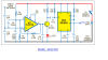
This is a mobile detector which detects pulses from the mobile phone transmission and the output of the first stage involving 3130 is given to the 555 which is wired as a monostable multivibrator.
 

Attachments

  • Untitled.png
    Untitled.png
    49.8 KB · Views: 230
What rectifies the Mobile Phone RF to create a shift in the output of the 3130?

(This is a brain-dead circuit)!
 
Last edited:
Thanks Mike and bychon
But then I have wired the circuit and its working....Its detecting the mobile signal, less range though.And sorry to ask but what did you mean by brain dead?
Bychon is it just an amplifier???? The article accompanying this circuit claims that it is wired as a voltage to current converter.And the inputs to both inverting and non inverting terminals are same except for a coupling capacitor.?
 
"Just an amplifier????" What do you think it is besides an amplifier?

Technically, when it amplifies voltage, current comes out, but one definition of a current amplifier is that a precise amount of current will be forced to travel in the feedback loop, and typically, that current is used to signal the next stage. This amplifier amplifies voltage, and the current that results is only dependent on the load (T1). The current that signals the next stage is not used in the feedback loop.
 
Last edited:
The RF detection part of this circuit is not so much designed, but rather something which by chance just happens to work.

The mobile phone signal is rectified by the base-emitter junctions of the input transistors in the 3130.

There is not even the pretence of a frequency selective tuned circuit on the input, or a basic RF detector.
Did someone say brain dead ? It is not far off that.

JimB
 
the antenna is 5inch log. so doesn't antenna wire and c1 make a frequency selection circuit( by series LC resonance circuit)
 
What rectifies the Mobile Phone RF to create a shift in the output of the 3130?

(This is a brain-dead circuit)!

I was trying to be funny. Using a microwave diode, and a proper tuned circuit between the antenna and the DC amplifier (the OpAmp), you could make an RF detector which is ~100 times more sensitive than this POC.
 
The opamp's input can be overloaded by nearly any radio frequency that has enough power. The radio output power of a cell phone is very powerful when it is near this lousy circuit. Cell phones work on many high radio frequencies so you do not want the input to be tuned to only one frequency.
 
Thanks guys now let me post the article accompanying the circuit.I have some doubts regarding the working.....
Article

An ordinary RF detector using tuned LC circuits is not suitable for
detecting signals in the GHz frequency band used in mobile phones. The
transmission frequency of mobile phones ranges from 0.9 to 3 GHz with
a wavelength of 3.3 to 10 cm. So a circuit detecting gigahertz signals is required for the
mobile bug.Here the circuit uses a 0.22μF disk capacitor (C3) to capture the RF signals
from the mobile phone. The lead length of the capacitor is fixed as 18 mm with
a spacing of 8 mm between the leads to get the desired frequency. The disk capacitor
along with the leads acts as a small gigahertz loop antenna to collect
the RF signals from the mobile phone Capacitor C3 in conjunction with
the lead inductance acts as a transmission line that intercepts the signals
from the mobile phone. This capacitor creates a field, stores energy and transfers
the stored energy in the form of minute current to the inputs of IC1.
This will upset the balanced input of IC1 and convert the current into the
corresponding output voltage. Capacitor C4 along with high-value
resistor R1 keeps the non-inverting input stable for easy swing of the output
to high state. Resistor R2 provides the discharge path for capacitor C4.
Feedback resistor R3 makes the inverting input high when the output becomes
high. Capacitor C5 (47pF) is connected across ‘strobe’ (pin 8) and
‘null’ inputs (pin 1) of IC1 for phase compensation and gain control to
optimise the frequency response.


Well the doubts are
1.How does the resistor R1 and capacitor C4 keep the non iverting terminal voltage stable?
2.How the capacitor connected across strobe and null input provide phase compensation and gain control?
 
Last edited:
JimB what do you say about the specifications of the capacitor C3 (which acts as a loop antenna) i.e the lead length ,spacing etc.Isnt that the design for frequency selectivity??Please correct me if Im wrong
 
datasheet here

Perhaps if you read the datasheet on the CA3130, it will give you clues about how it is used in your circuit.
 

Attachments

  • CA3130.pdf
    937.3 KB · Views: 283
1.How does the resistor R1 and capacitor C4 keep the non inverting terminal voltage stable?
R1 and R2 are a voltage divider that sets 0.52V at the non-inverting input of the opamp as a reference voltage. C4 filters it. Then without a signal the transistor is turned off and a signal causes the output of the opamp to go positive which turns on the transistor.

2.How the capacitor connected across strobe and null input provide phase compensation and gain control?
That is how old fashioned opamps were frequency compensated so that they do not oscillate at a high frequency where their phase shift is more than 180 degrees and the circuit has negative feedback. Modern opamps have the compensation capacitor built-in.
 
JimB what do you say about the specifications of the capacitor C3 (which acts as a loop antenna) i.e the lead length ,spacing etc.Isnt that the design for frequency selectivity??Please correct me if Im wrong

Using a .22uF capacitor as a tuned RF circuit for Ghz frequencies is about a stupid an idea as I have heard in a long time.
If it works at all, it will be dependant on the individual design of capacitor, the lead lengths of the capacitor, the layout and wiring on the circuit board.

Did someone say brain dead?

JimB
 
Status
Not open for further replies.

Latest threads

New Articles From Microcontroller Tips

Back
Top