Fluffyboii
Active Member
Hi,
I recently acquired my PIC16F1939 for driving LCDs for my watch project. I am hoping to fit it inside a wristwatch but if I can not do that I will just use large static LCDs to make a clock.
Since I could not find a DIP version of the chip in local shops and did not want to order one single chip online, I just bought the SMD version. To be more specific it is the 44-Pin TQFP package. There are PCBs to convert it into DIP package and I could buy one later but I thought I would design a converter myself and get it drilled on copper in my school.
This is my current PCB layout to convert this IC to something that can be put on a breadboard like the Arduino Nano:


There is 0.7 inch gap between the pins so this should go on a breadboard just fine.
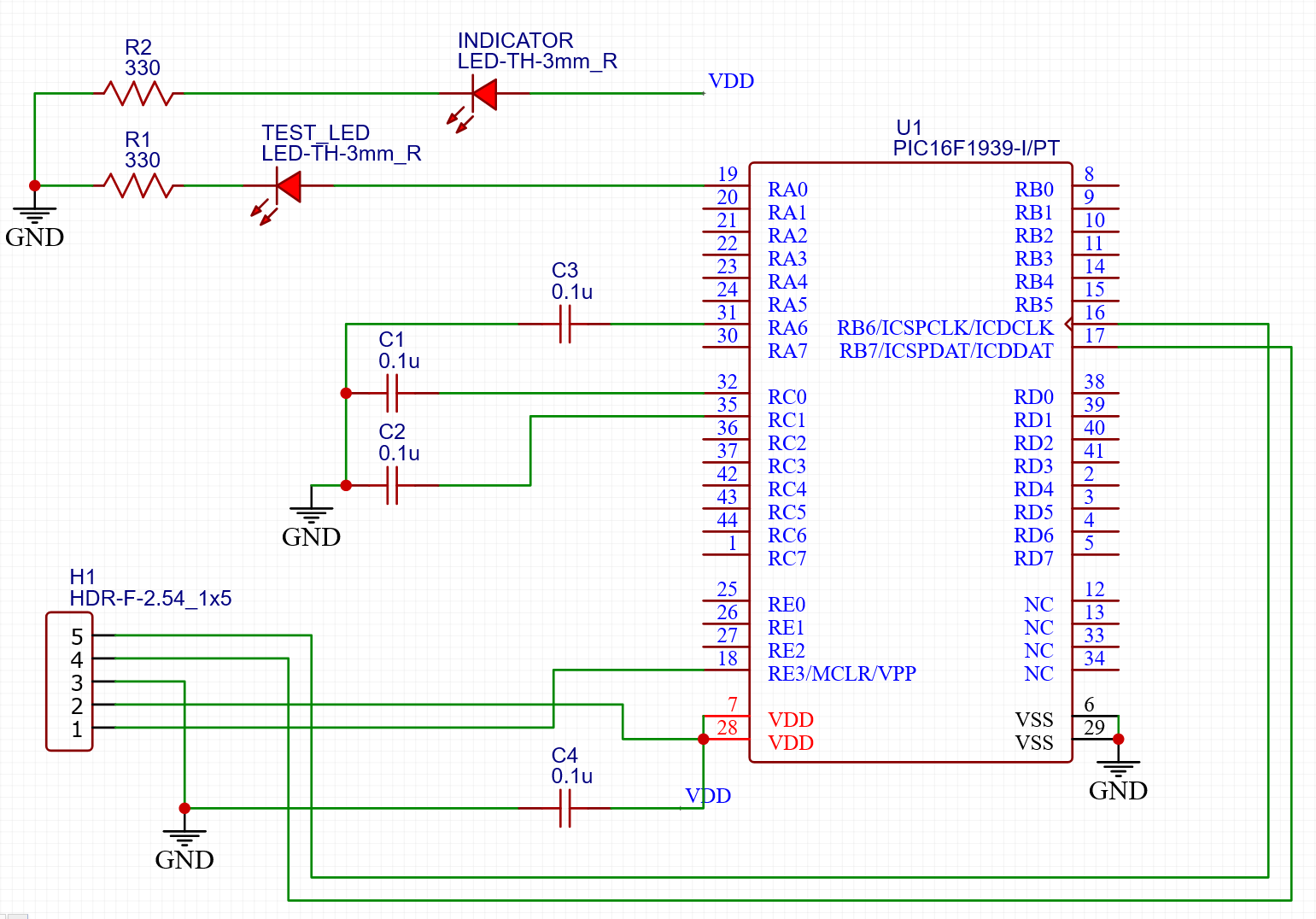
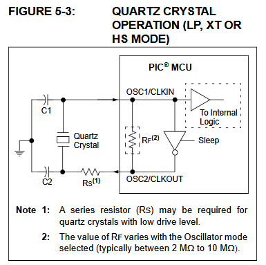
I was thinking of soldering one of my small 32678Hz crystals at the bottom of the PCB. C1 and C2 are for adding small capacitors from the crystal to ground. C3 is for the built in linear DC-DC converter. It is said to be optional to use a capacitor there but I decided to put it just in case (0.1 uF in datasheet). Thanks to the converter it should work between 1.8V and 5.5V. There are supercaps rated for 5.5V so I may go with a solar powered clock if I can keep the power usage low enough. C4 is regular decoupling capacitor. Quartz crystal is missing in the schematic as I could not find a suitable footprint. I will solder it in between RC0 and RC1 for Timer1 oscillator connection.

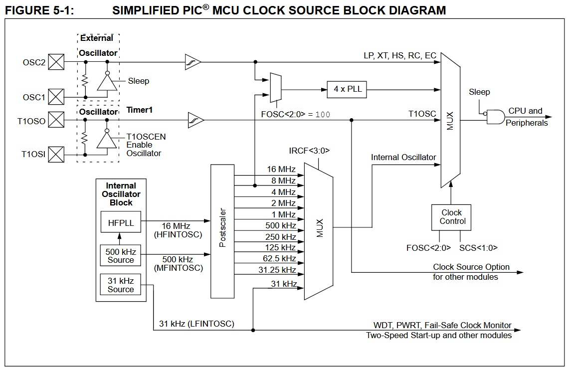
Datasheet says that Timer1 is especially designed to work with a 32678Hz quartz crystal to do time keeping. From what I understand Timer1 register can be used to count and wake CPU every second to update seconds. Also, this clock signal can be used as the main clock source of the mcu. Or built in clock generator can be used as well. Can I save power by running the mcu with a slow clock speed?

I wired the programming pins according to the datasheet to connect to a pickit. I saw one tutorial using a weak pull up resistor for V_PP/MCLR pin but I can not find it referenced in the datasheet. I have added an LED for power indication and another LED connected to the RC0 pin for no particular reason, at least I can use it to test blink code or something. My goal here is to use this board with breadboard to prototype my LCD watch stuff then remove the mcu to use it in the real think when I feel ready. Are there any glaring issues with the layout? I would like to ask since I never used a microcontroller before.
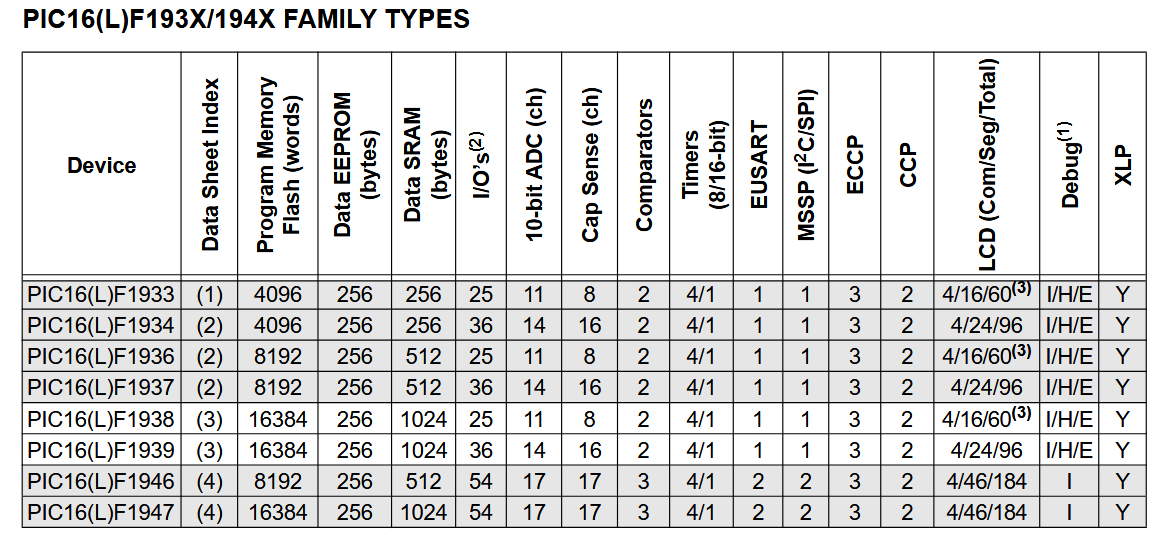
I could have picked up a F1933 instead I guess. F1939 is kind of overkill for my application as I will probably not use 16 segments pins. Only reason I initially chose it was because it had DIP version sold on online shop but I ended up buying the SMD version from local vendor anyway. Should have bought one DIP F1939 to breadboard with and a SMD F1933 to use in finished project.

I recently acquired my PIC16F1939 for driving LCDs for my watch project. I am hoping to fit it inside a wristwatch but if I can not do that I will just use large static LCDs to make a clock.
Since I could not find a DIP version of the chip in local shops and did not want to order one single chip online, I just bought the SMD version. To be more specific it is the 44-Pin TQFP package. There are PCBs to convert it into DIP package and I could buy one later but I thought I would design a converter myself and get it drilled on copper in my school.
This is my current PCB layout to convert this IC to something that can be put on a breadboard like the Arduino Nano:
There is 0.7 inch gap between the pins so this should go on a breadboard just fine.
I was thinking of soldering one of my small 32678Hz crystals at the bottom of the PCB. C1 and C2 are for adding small capacitors from the crystal to ground. C3 is for the built in linear DC-DC converter. It is said to be optional to use a capacitor there but I decided to put it just in case (0.1 uF in datasheet). Thanks to the converter it should work between 1.8V and 5.5V. There are supercaps rated for 5.5V so I may go with a solar powered clock if I can keep the power usage low enough. C4 is regular decoupling capacitor. Quartz crystal is missing in the schematic as I could not find a suitable footprint. I will solder it in between RC0 and RC1 for Timer1 oscillator connection.
Datasheet says that Timer1 is especially designed to work with a 32678Hz quartz crystal to do time keeping. From what I understand Timer1 register can be used to count and wake CPU every second to update seconds. Also, this clock signal can be used as the main clock source of the mcu. Or built in clock generator can be used as well. Can I save power by running the mcu with a slow clock speed?
I wired the programming pins according to the datasheet to connect to a pickit. I saw one tutorial using a weak pull up resistor for V_PP/MCLR pin but I can not find it referenced in the datasheet. I have added an LED for power indication and another LED connected to the RC0 pin for no particular reason, at least I can use it to test blink code or something. My goal here is to use this board with breadboard to prototype my LCD watch stuff then remove the mcu to use it in the real think when I feel ready. Are there any glaring issues with the layout? I would like to ask since I never used a microcontroller before.
I could have picked up a F1933 instead I guess. F1939 is kind of overkill for my application as I will probably not use 16 segments pins. Only reason I initially chose it was because it had DIP version sold on online shop but I ended up buying the SMD version from local vendor anyway. Should have bought one DIP F1939 to breadboard with and a SMD F1933 to use in finished project.
Last edited:

