Continue to Site

Welcome to our site!

Electro Tech is an online community (with over 170,000 members) who enjoy talking about and building electronic circuits, projects and gadgets. To participate you need to register. Registration is free. Click here to register now.

  • Welcome to our site! Electro Tech is an online community (with over 170,000 members) who enjoy talking about and building electronic circuits, projects and gadgets. To participate you need to register. Registration is free. Click here to register now.

Ground Loops / Multiple Net Pours / Grounding vias

Status
Not open for further replies.

ThomsCircuit

Well-Known Member
Im glad I decided to make this project. It looks simple enough but it does require design considerations that I dont fully understand. Currently China is on lock down so acquiring some parts is extremely slow. A project I submitted for fabrication to JLCPCB has been stalled in the delivery que for over a week so Ill focus on these issues here.

Vias.
I havent noticed them until i started this project. Now i see them on ready to purchase modules like this one. It was suggested that i add some around the ground track by pin 1 of MP2315. My PCB program does not have this feature so i would need to do this manually. Problem is i dont know how many, how big, or how close they should be. Trying to understand the many different vias but it can get confusing. It was suggested that a pour around a net would be better than adding an array of vias.
Screenshot 2022-03-23 at 22-42-57 Buck Step-down LM2596 Power Converter Module DC 4.0~40 to 1....png

---------------------------------------------------------------------------------
Ground Loops
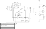
I know nothing about this. Well I cant say that. I do know the tracks should be as close as possible. This PCB is 30mm x 30mm. How do i tell if ive connected these in the right order? Do you need to see the schematic to understand if the PCB is optimally designed. If so I attached it.
POURS2.png

----------------------------------------------------------------------------------

Net Pours.
sometimes when you show someone a new tool they tend to use it for everything. Have i done that here? Do I have too many separate pours on this pcb? I mean tracks should be wide enough to provide the voltage required so why not surround that track (net) with a polygon and pour a big fat copper pour around it. Boom problem solved. Well I did that and then did another, and another, and another. So if you can make sense of my image ive got quite a few net pours for signal and current nets and then a ground pour. I colored a few nets for clarity.
The blue colored tracks represent the ground track. Its pour makes a continuous connection of every pad and through-hole. With wide and sufficient spokes. And then one huge GND plane on the bottom too.
The 12V is in a tan color (has no pour) Ive highlighted one net pour in grey.
If you look closely you can see the outlines of the other net pours. Im concerned I may not need every net to have a pour. I mean these pours place nets very close to one another right? Is that good for this buck module?
POURS.png
 

Attachments

  • Buck-S - Project-1.png
    Buck-S - Project-1.png
    104.8 KB · Views: 186
Regarding grounding loops:
From what i have read and can understand what not to do is connect components ground at multiple points. When I began designing a member showed me how to connect tracks. He advised not to have more than 2 points on any one pad. Basically you connect in then out. Try to avoid having a third track stemming from a component. I have done that here.
I also have no isolated ground planes like is shows in the photo on the top layer and the entire bottom is a ground plane as well. I am going to conclude that for this small project there are no grounding loop issues. I am still curious about using pours for signal and current tracks. Notably if I have too many or any un-necessary pours.

isolated ground.png

ground.png
 
Ran across a document (PDF) where the manufacture describes in detail how to design and layout a PCB with a particular set of components. They address placement, ground layers, and via stitching for a DC-DC boost to ground current source. Something similar to my project. Its worth reading as it explains in detail where to place supporting components and via stitching. I now know why its called stitching.
There are times when I would be presented with multiple suggestions from members of the forum about how to improve a project. While I want to implement all of them I sometimes have to choose one method over another. Ive learned that this does not mean that one members solution is better than another. It means that each member has different experiences. They present answers and advice based on what has worked for them in the past. Ive also learned that components and ICs even those of the same purpose and function will have different methods for dealing with noise, and maximizing performance.
After reading the article I made some changes to my PCB. I feel that they apply to my project.
I placed 2-3 ground vias near each capacitor. The manufacture states the following.
"..in order to keep the parasitic inductance and resistance of the connection lower than 5% of their internal ESL and ESR"
Capacitor Vias.png

But this line goes against what ive been taught here by the group.
"Capacitor connections shall be made with the shortest traces possible, avoiding thermal reliefs." No thermal relief?
Im sure they have a vaild reason for doing so but unless someone here can explain why Im going to keep the relief spokes.
Ive also looked over my schematic and relocated C4 closer to L1 and altered the track so it connects directly to L1 instead of L2. How much of an improvement that will do in unknown but it is logically correct.
The article also suggest that the two inductors showed be further apart from each other when one is being used as a noise filter.
Happy reading.
 
avoiding thermal reliefs
I do not use thermal reliefs. These small parts do not have a heatsink other than the coper they are soldered to.
First example is the IC which has a heat pad under the part that needs to connect to a large piece of copper to pull out the heat. Inductors and capacitors and resistors will run cooler if they have a good connection to copper. The whole point of a thermal is to stop heat from getting out.

Some of my supplies, I am switching 100 amps and I want the lowest resistance possible in the solder connection to copper.

It will take more time to solder parts well connected to copper. I often solder the board in an oven that heats the entire board at one time. Or I use a hot air gun to heat the area around a part.

Wow you did the board single sided. The cost of a double sided board is the same. I might fill the back side with ground. I use VIAs under the IC to carry heat to a copper heatsink on the bottom side.

If you solder in a oven ... no problem. If you hand solder with a iron, make the pads a little longer. In KiCAD there are often two pad options for most parts. "normal" and "hand solder". The later have extra long pads for a solder iron to hit.
 
Wow you did the board single sided. The cost of a double sided board is the same. I might fill the back side with ground.
It is double sided. I mean i have 2 components on the opposite side and the entire bottom is a ground plane. I found out the JCPCB will do a 4 layer board 50x50mm at the same cost as a 2 layer board 100x100mm. Perhaps using a layer for the +Voltage Source.
I might fill the back side with ground. I use VIAs under the IC to carry heat to a copper heatsink on the bottom side.
I read about that. My version of DS has no ability to populate an area with vias so i would manually add them. I was looking for what the via size, its hole, and how far to space them would be. Based on what i have read a vais hole is .20mm and i saw a heat sink where they were spaced 3mm apart. Id like to add one such heat sink to the bottom of L2 as i understand it can get hot under extreme input / output conditions.
In KiCAD there are often two pad options for most parts. "normal" and "hand solder". The later have extra long pads for a solder iron to hit
cool feature. I often wait for the components to show then compare to the footprints and adjust them for my sausage fingers.

Design spark (free) also does not do tented vias so i had to rearrange an SMD led so the vias were not directly on the pad.
 
I was looking for what the via size, its hole, and how far to space them would be.
Probably you can make a VIA any size you want.
jlcpcb Drop down to "drill hole size". They show the smallest and largest holes and vias. and spacing. I often do not use the smallest hole. Look at what they can and cannot do.
 
OK tell me i did this correctly or not. I used Design Spark and added a heatsink.
1) created the appropriate size via (.30mm hole x .80mm) and spaced them as advised (1mm apart)
2) assigned the vias to the components net.
3) Added a POURED SHAPE* to suit the component. assigned to the same net, moved it to the bottom layer.
*a poured shape is different from a copper pour area
-----------------------------------------------------------------------------------
In this project L1 is a filter so a heatsink is only needed for L2

heatsink1.png
heatsink2.png
 
Last edited:
Inductors and capacitors and resistors will run cooler if they have a good connection to copper. The whole point of a thermal is to stop heat from getting out.
While I try to add a copper area on the bottom layer and vias DS throws an error that equates to "tented vias" and thats not allowed. I mean they are but not in DS. It only works when the copper area and via share the same net. And i dont know if thats what supposed to be done. I have a few questions posted with the DS forum in hopes that they help me figure it out. If not i can just use a small number vias linked to ground with no copper shape on the bottom.
I do not use thermal reliefs. These small parts do not have a heatsink other than the coper they are soldered to.
I can appreciate now why it is important to thoroughly understand your circuit. To know where the heat will be, and choose to widen the tracks or use copper pours to control it. If this project was not associated with such an in depth article I would have no clue which to use. I have also learned that wide traces and copper pours may appear to acomplish the same thing but there are subtile differences that make them very different.
 
Last edited:
From what i have read further reguarding moving heat away using copper pours is there effectiveness is highly opinionated. And while there is lots of discussion on spacing, size, and the number im not finding much on how to apply it in the PCB software. So I still have a few questions on how to add vias as a heat sink. And I mean in Design Spark. Specifically the copper shapes and the vias. What net would you attach them to? Ground, the components, signal net?
If i had the choice i would choose none. but DS does not allow it. (throws errors) Id create the top and bottom pours and place the vias in the void. Save it as a group item and put it in place. Any other pours that are connected to nets and grounds would wrap around it. It would be an island. I think it would be better if i could remove the bottom solder mask too. Thus exposing the copper.
This image shows what I have done. The copper shapes and the array of vias are connected to the signal net on L2. The vias do not show because of the color limitations of DS

heatSink With vias.png
 
Reguarding Multiple pours on one layer.
I was concerned about the gap between the pours.
Its perfectly fine to have multiple copper pours around nets on one layer without creating any signaling issues unless your circuit has RF signals.
 
The manufacturer of the MP2315 gives a sample PCB layout on page 13 of the datasheet. I'd recommend studying it and using it as a guidline.

As you've said, every engineer has their own design philosophy and history based on whatever similar projects they've worked on. When you have knowledge from the chip designers themselves, that should weigh in heavily.

https://www.monolithicpower.com/en/...atasheet/lang/en/sku/MP2315S/document_id/981/
 
The manufacturer of the MP2315 gives a sample PCB layout on page 13 of the datasheet. I'd recommend studying it and using it as a guidline.
I remember you making this suggestion. At the time I had pretty much no idea how to interpret most of it but now after i have had time to explore optional methods I see what you are referring to and i am pleased i do understand what i am seeing.
I can see there are 2 series of via arrays on the ground plane. I am thinking that they are to help with heat. They are nearest pins 3 and 5. SW and BST

Now the issue i was having was adding a heat sink under the inductor L1 (See post 10)
That would be what net do i attach the pours and vias to.

Vias on ground plane nearest pins 3 & 5
via arrays.png
 
Ive redrawn the PCB to take advantage of the manufactures layout suggestions. I only relocated the track to pin 3 as it was too close to pin 8.
I also did what i could to place all the components where they need to be i relation to the IC and have the grounds of those components in the same general location.
The current mirror at the top is just for an led. Its ground connection is through a via that is on the bottom copper pour layer.
I now have a clear understanding of copper pours and via arrays. I still dont fully understand on identifiying potential ground loops and avoiding them. But i do think this layout is an improvement.
NEW LAYOUT.png
 
For heat transfer, put an array of VIAs within and around each component connection pad.
They need to be connected to each pads respective net and copper areas in the same net as the pad, on other layers.
 
For heat transfer, put an array of VIAs within and around each component connection pad.
They need to be connected to each pads respective net and copper areas in the same net as the pad, on other layers.
Ok. Im working on that. Of course i have a question regarding spokes.
I get the concept of using vias for heat transfer and a means to join top and bottom planes for better conductivity. For these non soldering purposes i set the spokes to none and set the via to non isolated as shown on the right.
On the left is where i use via to connect a track to ground on the bottom layer. Since im not soldering anything to it does it need spokes? Can i just set it as the others?
via with spokes.png
 
Of all the projects i have attempted this has been the most educational. This group and especially its members are both knowledgeable and patient with new recruits like myself. And for all that I thank you.:D
Unlike other projects I have had to consider component placement, heat transfer, placement in relation to other components, grounding loops, copper pours, and vias arrays. And as a bonus i got a current mirror that powers an led from a range of voltages.
Below is hopefully the final version of my buck converter. Shown with a few copper pour areas filled.
final pcb.png
 
For heat transfer, put an array of VIAs within and around each component connection pad.
They need to be connected to each pads respective net and copper areas in the same net as the pad, on other layers.
Ive re-read this and may have missed an important step. "on other layers"
since all components are SMD all nets are on the same layer and the vias are through hole would there be an advantage (heat wise) to put a small copper pour or pad on the bottom layer and assign it the same net at that on the top layer? Or just leave the bottom as a ground pour.
Hope this image helps explain.
LAYER STACK.png
 
If heatsinking is absolutely vital, then try to make the copper area on other layers the same as for the component or even larger, and link them with a grid of VIAs.

With ICs that need that style of cooling the heatsink pad(s) are often grounded so not a problem, but for other things then make an island in the ground plane; just try to ensure it has a decent ground area around it still.
 
With ICs that need that style of cooling the heatsink pad(s) are often grounded so not a problem, but for other things then make an island in the ground plane; just try to ensure it has a decent ground area around it still.
Thank you. I wanted to be sure I knew how it was done. The manufacturer doesn't say one is needed but it does say if the placement of the other components can / will affect the chips performance. The inductor does get hot. I put an array under it. Ill read up on how hot it can get.
I have seen on pcbs large pads on the bottom layer under a component with no solder mask. I think they serve a different purpose though. Like when the components pad is covered by the component so a paste is applied then it is heated from underneath to melt the solder.
 
Last edited:
Status
Not open for further replies.

Latest threads

New Articles From Microcontroller Tips

Back
Top