Continue to Site

Welcome to our site!

Electro Tech is an online community (with over 170,000 members) who enjoy talking about and building electronic circuits, projects and gadgets. To participate you need to register. Registration is free. Click here to register now.

  • Welcome to our site! Electro Tech is an online community (with over 170,000 members) who enjoy talking about and building electronic circuits, projects and gadgets. To participate you need to register. Registration is free. Click here to register now.
Status
Not open for further replies.
Hello people!
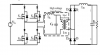
I am trying to find a gate driver for IGBTs for a current-source full bridge topology. The main difference between current-fed and normal voltage-fed converters is that due to a boost inductance at the input, there should always be a path of current flow. So, as we give dead time in voltage-fed converters, here we have to give overlap time. However, I am facing a lot of doubts and problems. Some of them are:
1. How will I use de-sat protection?
2. How will I ensure other protection schemes such as over voltage?
3. How will I ensure that there is always some path for conduction and current never gets chopped?
I would be highly obliged if one can suggest me a good IC.

Edit: Also How will it help if I use MOSFET instead of IGBTs as no Desat protection is used for MOSFET?
 
Last edited:
current-source full bridge topology
Is this what you are doing?
2018-09-17-192647_1184x624_scrot.png
 
Many years ago I did a MOSFET, half bridge version.
I just noticed what I did was different. I moved the input inductor to the output.
The 1/2 bridge reduced the silicon and reduced the turn ration on the transformer.
It was one of my best. Ran cool. I almost shipped it with out heat sinks.
 
Many years ago I did a MOSFET, half bridge version.
I just noticed what I did was different. I moved the input inductor to the output.
The 1/2 bridge reduced the silicon and reduced the turn ration on the transformer.
It was one of my best. Ran cool. I almost shipped it with out heat sinks.
I did not understand.. What does moving input inductor to output mean?
 
Sir, Please help me. Only you can help me
Suggest you start with showing what exact topology you have in mind, how you expect it to work, what are the input/output parameters etc. Without that it is very hard to give you any reasonable advice.
 
Suggest you start with showing what exact topology you have in mind, how you expect it to work, what are the input/output parameters etc. Without that it is very hard to give you any reasonable advice.
Vout =500V
Vin=28-42 V
Iout=2A.
Topology is a full bridge isolated boost with passive snubber.
 
How will it help if I use MOSFET instead of IGBTs
Look at the voltage loss across the two types of transistors. I think the MOSFET is better at low voltage applications.
You need to find a IC that works like you want. That will solve many problems. If you try this with a micro computer then you will need to have at least one top and one bottom transistor on all the time.
1000 watts, Vin = 25V @ 40A average.
I think you need to find several papers on this and read them.
 
Vout =500V
Vin=28-42 V
Iout=2A.
Topology is a full bridge isolated boost with passive snubber.
What is the highest peak plus transient voltage that your switches will see?

In my opinion, unless they're seeing 600V or more, mosfets are probably a better choice than IGBTs. There are of course, multiple factors involved in the decision.
 
1. How will I use de-sat protection?
No desat should ever occur, because there is no possibility of hard shootthrough that would cause the igbts to go out of saturation. Unless you stop driving the swithces and keep them on, then you will have a lot of troubles.
2. How will I ensure other protection schemes such as over voltage?
Do you mean overvoltage on the input, or spikes caused by the switching action?
3. How will I ensure that there is always some path for conduction and current never gets chopped?
I would be highly obliged if one can suggest me a good IC.
Like Ron said, allways one top and one bottom switch has to be on. The cycle of ON devices should be:
S1 S2 S3 S4
S1 S3 (D1 D3)
S1 S2 S3 S4
S2 S4 (D2 D4)
 
I think you want to make A.
About 30 years ago I made B. Where a simple PWM boost drives one MOSFET . A simple D-flip flop divides the frequency by 2 and drives the gates. The 4-MOSFETs switch when the first MOSFET is on. So for the 4-mosfets there is no AC losses. They switch with no voltage on the Drain.
Because I must keep the cost down, I made C with only 3 transistors.
1537307753764.png

I made a "gate" drive that is very simple. It will take some time to remember how.
 
I found (D) in a old pile of prototypes. I used a simple boost PWM IC. Any time the IC wants to turn on the FET it turns on both FETs. When the IC turns off the FET one stays on. See the two OR gates and the toggle flip flop.
1537312322879.png

I don't know if this helps you. I think (D) could be changed to a full bridge.
 
No desat should ever occur, because there is no possibility of hard shootthrough that would cause the igbts to go out of saturation. Unless you stop driving the swithces and keep them on, then you will have a lot of troubles.
I did not understand Sir. Can you please ellaborate a bit.
Do you mean overvoltage on the input, or spikes caused by the switching action?
Yes. Also, Overcurrent.
Like Ron said, allways one top and one bottom switch has to be on. The cycle of ON devices should be:
I figured that logic out. but protection is when due to some condition the logic fails,
 
I did not understand Sir. Can you please ellaborate a bit.
Not sure what is the trouble. Desturation occurs when the current through IGBT is so high that the driving internal fet cannot supply enough current to the base of the bipolar transistor, and the transistor is then no longer in saturation. This leads to increas of Vce, and subsequent faiulre of the igbt due to excessive power dissipation.

Usually this happens in one half of the bridge, when both igbts are on at the same time - a shoot-through. Because the power rail is a hard voltage source, the current through the two igbts rises very fast and usually destroys them, unless the driver detects that and shuts the igbt off.

In your current fed topology this is not the case, becase basically constant current flows there, and when both igbts are on at the same time, it is still only that current flowing and you don´t get the sharp increase in current as in voltage fed topology.
 
Status
Not open for further replies.

Latest threads

New Articles From Microcontroller Tips

Back
Top