Continue to Site

Welcome to our site!

Electro Tech is an online community (with over 170,000 members) who enjoy talking about and building electronic circuits, projects and gadgets. To participate you need to register. Registration is free. Click here to register now.

  • Welcome to our site! Electro Tech is an online community (with over 170,000 members) who enjoy talking about and building electronic circuits, projects and gadgets. To participate you need to register. Registration is free. Click here to register now.

feedback in amplifiers help..

Status
Not open for further replies.

wakoko79

New Member
can anyone show me links for tutorials/ videos concerning feedback used in bjt amplifiers?

i already perused links in the sticky section..

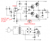
i know the 4 topologies, but i dont know how to place it in circuits... im specially interested in series shunt topology, since what i need to do is to amplify a signal to a 8ohm speaker.

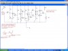
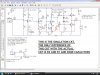
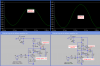
i already made an amplifier circuit,, but it is without feedback so its pretty crappy. i dont really know how to improve it.. pls help... thanks!!
 

Attachments

  • 10012010.jpg
    10012010.jpg
    354 KB · Views: 184
  • ckt.JPG
    ckt.JPG
    126.4 KB · Views: 214
Your "amplifier" has too many coupling capacitors. Real audio amplifiers are direct DC-coupled so that the DC gain is 1 with negative feedback. AC gain reduces the negative feedback and is made with two resistors and one capacitor.

You don't need a tutorial. Simply look at the millions of audio amplifiers on the internet.
 
Order this book. $2.50US is a bargain (you'll pay more for shipping) There is a great treatment of feedback, as well as alot of great information on amplifiers. Many of us used this as a text in our university studies. I still use mine for reference, 15 years later...
 
Last edited:
This circuit is an 18W amplifier from Red Circuits. It is the second link for "Audio Amplifier" in Google. The first link is the same amplifier with a fairly complicated tone control.
It uses an opamp (are you the guy whose teacher said to use an opamp?) and has negative feedback.
 

Attachments

  • 18W amplifier.PNG
    18W amplifier.PNG
    18 KB · Views: 216
no.. actually my teacher restricts us to use only bjt's.. i wish i could use opamps, it would have been much much easier to implement feedback with it.. the other teachers allowed it, my teacher is an ass..
so i understand that the feedback network is connected to the output just before the speaker.. should i connect its other end to the very first input of the first bjt? or should i place it on a different stage?


i think i should take out the emitter follower, it pretty does nothing in the ckt, bad idea from my classmate. =(

Order this book. $2.50US is a bargain (you'll pay more for shipping) There is a great treatment of feedback, as well as alot of great information on amplifiers. Many of us used this as a text in our university studies. I still use mine for reference, 15 years later...
thanks.. ill look it up in the lib.. or try to find it domestically..

thanks again.. this forum is really helpful, and i get a reply within a day=)
 
I don't understand why your teacher expects you to design or copy an amplifier that uses transistors when you do not understand the basics about transistors. Didn't your teacher teach about how transistors work and how to properly bias them? Your transistors have a fairly high collector-emitter current but a current that is too small in the divider that biases them. Then the transistors with low current gain will not have enough base current and temperature changes will also affect them.

Weren't you taught about amplifiers that use negative feedback? If you connect the feedback to the wrong location then it is positive feedback which makes a square-wave oscillator instead of an amplifier.

Make the amplifier DC-coupled. Usually an amplifier has a differential input so that the input signal goes to one transistor and the negative feedback connects to the other input transistor.
 
I'm here again.. I already figured out how to employ negative feedback in my ckt. my ckt is doing well in simulation but not so good in actual testing.
here are the notes i took:

1.) cap C7 (9v to ground). when i tried to make this 1mf, the voltage in the voltage source went down. i immediately turned it off. it was about ~7V. its supposed to dampen the ripples in the source right? not only that, when i increased C7 from 100uf to 200uf, the gain at the output got a little bigger. that's why i tried to make it even fatter(1mf). can anyone tell me why is this happening?

2.) the output was REALLY DISTORTED. but after about 15 to 20 seconds, the output slightly smoothens out. what really bothers me is that when i adjusted bias resistors R13 and R14(i momentarily turn them to minimum then turn them up again) the distortion before just vanishes. i forgot to take a picture of the distorted waveform, sorry. I don't know if it was just the scope i was using though, it was semi old and i havent got the permision to use the new ones(still in the package box.)
I'm afraid that when i take this to my teacher, he wont check my workbecause of this.

3.) minor thing: the 2n2222A and 2n2907A i use are in the round metal casings. the 2n2222A looks pristine, the 2n2907 is like.... burnt... at first it was a little yellowish. now its more brown than yellow. do you think the 2n2907a is hogging most of the current? i suspect that this has something to do with the potentiometer biasing i made, sometimes the biasing just go too low, or too high.. btw, 2 burned the first 2n2907.. i tried biasing with 100k pots at that time. i dont know what happend, but the 2n2222A was still intact.

4.) In SIMULATION: if R9 is lower than R10 (e.g. R9=33kohms R10= 100Kohms), the output at the collector of Q3 distorted at the upper part. i tried bypassing R10 (i guessed that the AC impedances has something to do with the distortion, i was wrong) but it was still distorted.

5.) in SIMULATION of the ACTUAL CKT: the frequency response tells me that f>1kHz has a pretty stable gain, in reality, it has not.


i guess i should tell you the requirements:
-> 0.2Watt rms at the output (~1.8v peak)
-> i use 8ohm 0.5watt speaker
-> no distotion
-> from 25Hz to 20kHz
-> suggested use of preamp stage and voltage driver(i have no idea what the hell voltage driver means, maybe amplify the voltage to levels greater than line voltage?)
-> BJts only. no opamps/jfet/mosfet


enlightment please!!! thanks!


PS:
Your transistors have a fairly high collector-emitter current but a current that is too small in the divider that biases them. Then the transistors with low current gain will not have enough base current and temperature changes will also affect them.
pls. enlighten me about this.. all i know is that i have to compute for the thevenin equivalent of the biasing network then compute accordingly to get the wanted base voltage bias.. i dont know about the currents...


can anyone tell me where to get a more precise model of a speaker? the 8ohm resistance just can model it. thanks!!
 

Attachments

  • actual ckt.JPG
    actual ckt.JPG
    110.4 KB · Views: 158
  • sim ckt.JPG
    sim ckt.JPG
    122.3 KB · Views: 160
  • @100Hz 1.47V.jpg
    @100Hz 1.47V.jpg
    387.5 KB · Views: 169
  • @20khz 4.25V.jpg
    @20khz 4.25V.jpg
    373.1 KB · Views: 167
I'm here again.. I already figured out how to employ negative feedback in my ckt. my ckt is doing well in simulation but not so good in actual testing.
It is still AC-coupled. Good modern amplifiers are DC-coupled.

1.) Cap C7 (9v to ground). When I tried to make this 1000uF, the voltage in the voltage source went down. I immediately turned it off. It was about ~7V. Its supposed to dampen the ripples in the source right? Not only that, when I increased C7 from 100uf to 200uf, the gain at the output got a little bigger. That's why i tried to make it even fatter(1000uF). Can anyone tell me why is this happening?
The little 9V battery is old and has a fairly high internal resistance. The fairly high supply current of the amplifier causes the 9V to drop (because of the voltage loss in the internal resistance of the battery) and produces ripple. A big capacitor across the battery is a filter and smoothes out the ripple.

2.) The output was REALLY DISTORTED. But after about 15 to 20 seconds, the output slightly smoothens out. What really bothers me is that when i adjusted bias resistors R13 and R14 (i momentarily turn them to minimum then turn them up again) the distortion before just vanishes.
Your Q3 has a very high gain. It is amplifying temperature differences. The old battery voltage also drops after a few seconds and Q3 is also amplifying the difference. But the other transistors have very low gain. Spread out the gain at each transistor so that one does not amplify temperature and supply voltage changes as much. If the circuit is DC-coupled then temperature and supply voltage changes will have a very small effect because the negative feedback will cancel them. Since your circuit is AC-coupled then it has no DC negative feedback.

3.) minor thing: the 2n2222A and 2n2907A i use are in the round metal casings. the 2n2222A looks pristine, the 2n2907 is like.... burnt... at first it was a little yellowish. now its more brown than yellow. do you think the 2n2907a is hogging most of the current? i suspect that this has something to do with the potentiometer biasing i made, sometimes the biasing just go too low, or too high.. btw, 2 burned the first 2n2907.. i tried biasing with 100k pots at that time. i dont know what happend, but the 2n2222A was still intact.
Pots are a very poor way to bias the output transistors. If you used a Vbe-multiplier transistor instead of the diodes and DC-coupling like most amplifiers then there would not be a problem.

4.) In SIMULATION: if R9 is lower than R10 (e.g. R9=33kohms R10= 100Kohms), the output at the collector of Q3 distorted at the upper part. i tried bypassing R10 (i guessed that the AC impedances has something to do with the distortion, i was wrong) but it was still distorted.
When R9 and R10 are each 200k, the current in them is only 22.5uA. The base current in Q3 is 12.5uA to 37.7uA. The divider current should be 10 times the base current so your resistor values in the divider are way too high so the hFE of the transistor and the temperature affect the biasing very much.
Since the emitter resistor values for Q3 are very low then it has a very high DC gain that also affects the biasing very much.

5.) in SIMULATION of the ACTUAL CKT: the frequency response tells me that f>1kHz has a pretty stable gain, in reality, it has not.
The high capacitance of the tracks and wiring on your breadboard reduce high frequency response. The failing battery voltage probably causes the gain to slowly drop. Use a brand new name-brand 9V alkaline battery, or a regulated 9V power supply.

Can anyone tell me where to get a more precise model of a speaker? the 8ohm resistance just can model it.
An 8 ohm speaker is 8 ohms at very low frequencies and at a few frequencies above its resonant frequency. At resonance it is about 60 ohms and since a speaker is inductive then its impedance rises at high frequencies and at 20kHz is as high as 400 ohms.
But an audio power amplifier has plenty of negative feedback that causes its output impedance to be 0.04 ohms or less. Then the changes in the speaker's impedance do not matter.
 
The little 9V battery is old and has a fairly high internal resistance. The fairly high supply current of the amplifier causes the 9V to drop (because of the voltage loss in the internal resistance of the battery) and produces ripple. A big capacitor across the battery is a filter and smoothes out the ripple.
i forgot to tell that i am not using a battery,its a power supply, loadstar.

so how can i dc couple? remove coupling capacitors right? then compute accordingly the q-points. Should i also remove the ac coupling in the output stage?(C4 and C5?)
 
Fot the last 50 years, nobody has made an audio power amplifier with C4 and C5 like in your circuit.
There are many amplifier tutorials on the internet and only one (the very old one you found) shows it.
You should look at the thousands of amplifier schematics on the internet to see that they are all DC-coupled. You should also look at the hundreds of power amplifier IC schematics and all are DC-coupled.
 
what is the problem with c4 and c5? are they too big? they are just coupling capacitors tight? I'm still an undergrad so i dont know what else might these capacitors do. i can only think of their charge time and them being coupling capacitors, nothing more..

i just want to pass this project and be done with it.. ill just study it when i have more time, maybe at the summer break... just please help me do the job >.<
 
Since you want to be done with this project without looking at the hundreds of better amplifier circuits on the internet, I corrected your circuit so that the output transistors are DC-coupled from the driver transistor and added some negative feedback. I did not adjust the voltage gain.
Usually the two diodes are replaced with an adjustable Vbe-multiplier transistor that is bolted to the heatsink of the output transistors for thermal feedback.
Usually the output transistors have low-value emitter resistors to equalize their differences.
 

Attachments

  • very simple power amplifier.PNG
    very simple power amplifier.PNG
    38.1 KB · Views: 188
Last edited:
i tried this on simulation, it is awfully distorted... how is that?
Of course it is distorted, it is a very simple circuit.
The 1k resistor that applies base current to the 2N2222 output transistor does not supply enough current when the output swings high. Increasing the current by reducing the value of the 1k resistor will reduce the voltage gain that is already very low. So, I added a resistor in series with the 1k resistor and added a bootstrapping capacitor so that the base current for the 2N2222 transistor stays constant as the output swings high. I also biased the circuit a little better by increasing the value of the 3.3k resistor. Now the distortion is reduced and the voltage gain is increased.
 

Attachments

  • sim simple amplifier.PNG
    sim simple amplifier.PNG
    43.3 KB · Views: 162
Of course it is distorted, it is a very simple circuit.
The 1k resistor that applies base current to the 2N2222 output transistor does not supply enough current when the output swings high. Increasing the current by reducing the value of the 1k resistor will reduce the voltage gain that is already very low. So, I added a resistor in series with the 1k resistor and added a bootstrapping capacitor so that the base current for the 2N2222 transistor stays constant as the output swings high. I also biased the circuit a little better by increasing the value of the 3.3k resistor. Now the distortion is reduced and the voltage gain is increased.

Can you make the ciruit that you have there louder without making a lot of distortion?
 
Can you make the ciruit that you have there louder without making a lot of distortion?
No.
The supply voltage limits the output voltage swing. Therefore the max output power at clipping is about 0.46W. A cheap clock radio has more output power.
If the power supply voltage is increased then the output power would be higher but the little output transistors would be damaged by the extra current and heat.

Semiconductor manufacturers make more than 100 inexpensive amplifier ICs made for car radios with an output power of 14W at clipping into a 4 ohm speaker.
 
i think we are required to make a preamp stage (about hundred millivolts output) and a voltage driver (few volts peak to peak output). do you think i can do what i did in my previous ckts here? i mean distribute the gain to 2 stages? i'll try to do this at home though, im in a cafe now..

this will be hell for me in the documentation. we're only taught of feedback with CE CB and CC topologies. your ckt includes the feedback in the output stage, so computation will be hell. but i think i can do this!! gogogo! but if you ALREADY computed for feedback gain and the alpha beta stuff or causal equations.. it will be much help... just if you already have them.. i don't want to be a burden to anyone hehe.

audioguru. can you pls explain briefly how and why q1 is placed like so? again, we're only taught of CC CE CB topologies. i believe q1 is arranged as CE amp with Rc as load right? i just saw the same arrangement in my exam this morning (ramp generator) and im completely baffled with that particular question since i only know the basic bootstrapping RC transistorized ckt and the problem includes some part like q1..

going back.. can you also explain why the bypass(bypass=bootstrap right?) capacitor is placed like that? pls dont flame me for being so noob=) ill try to solve this ckt whn i get home and after some rest though/..

i understand that you included some explanation, i just cant read them now, im in a hurry.. ill read later.. thanks=)
 
My circuit has low gain because a transistor amplifier with high gain has terrible distortion. The negative feedback reduces the gain which reduces the distortion. Use a preamp to increase the gain instead of reducing the amount of negative feedback.

The first transistor of my 3-transistors very simple power amplifier circuit is common-emitter. Its base is biased by the negative feedback resistor in a voltage divider so that the output DC voltage is half the supply voltage for the max symmetrical output swing.
It is complicated to calculate the voltage gain because the circuit is so simple. I have the formula on my hard drive but never used it since I never use this awful simple circuit. If the input had a differential pair of transistors then the voltage gain is simply the ratio of the feedback resistors.

The bootstrap capacitor allows the base voltage of the NPN emitter-follower output transistor to swing up above the supply voltage for a high output level (my sim shows the output swinging to at least +7.5V) . Without the bootstrap capacitor, as the output swings positive then the current in R3 becomes less so the NPN output transistor does not go high enough (my sim shows the output swinging to only +6.5V).

If you reach down and pull up on your bootstraps then they lift you off the ground and your boots will be off the ground so they lift your arms up that are pulling your boots up. Up you go! It is magic but it works in electronic circuits because the boostrap capacitor has a constant DC voltage across it and when the output swings high then the capacitor pin above the base of the NPN output transistor swings high the same amount which makes the base voltage swing higher than the supply voltage with plenty of base current.
 
Last edited:
Status
Not open for further replies.

Latest threads

Back
Top