Electro Tech is an online community (with over 170,000 members) who enjoy talking about and building electronic circuits, projects and gadgets. To participate you need to register. Registration is free. Click here to register now.
Welcome to our site! Electro Tech is an online community (with over 170,000 members) who enjoy talking about and building electronic circuits, projects and gadgets. To participate you need to register. Registration is free. Click here to register now.
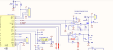
R9 only conducts transient current into C4 , so at DC it exactly like a voltage follower.
.
If U2B out = U2A+in, then
all +/- input in both U2A,B and U2B output will be at the same Vdc = Icoil / R14. This loop is not necessary unless scaling of constant current is desired.
Due to the coil inductive voltage changes with current ramps, we expect U2A-out to be the derivative with current. But from the square law of the FET Vgs control of drain current into R7 when Vgs is above Vt (aka. Vgs(th))
Thus U2A-out transfer function will be the square root of the derivative of Icoil when it is above Vt.
It is important to minimize all cable capacitance to the coil so that the self-resonant-frequency (SRF) does not cause the circuit to amplify spectrum near this from an impulse or step function..
Yes, but its sole purpose is to work with C4 to rolloff the feedback at higher frequencies, to improve the loop stability and reduce the chance of circuit oscillations.
An AC Bode plot of the circuit will likely show some peaking or instability in the response without the capacitor.
The DC path is like this. When the output of U2A goes up, Q1 increases lets more current through. The increased current flows through R14 so there is more voltage at TP6, so more voltage at the inverting input.
There are two feedback paths. The AC path is through C4, the DC path what I described in post #9.
R9 is in the circuit to increase the impedance of the DC feedback, so that C4 can be a much smaller value, and so that the output of the op-amp is not overloaded by the combination of C4 and R14.
No, I meant the DC feedback. Increasing the impedance of the DC feedback allows the AC feedback to have a similar impedance at the chosen cross-over frequency.
R9 & C4 form an LPF for the current feedback from the 1 Ohm resistor. C4 & R9 also form a high pass filter from the op-amp output so that fast feedback Lee the circuit from oscillating.
R9 & C4 form an LPF for the current feedback from the 1 Ohm resistor. C4 & R9 also form a high pass filter from the op-amp output so that fast feedback Lee the circuit from oscillating.
C4 integrates any difference between I sense in thru R9 and I sense out from uC DAC. Improved stability is the effect with a 10 ms time constant ~ C4||R7
Yes, any DC offset is corrected by the integrator C4 with the Gate R7 being the highest series R in the shunt across C4. The uC DAC sets the desired current , the 1 ohm senses it and the integrator FET driver provide the error correction to match the input from the DAC (DC or AC within integrator BW ) which attenuates any coil cable LC resonance, if that is a much higher f.
We do not know the LC parameters but the 1 ohm is power limited for current. e.g. << 0.25A for 1/4W or 5A for 5W. @ 150'C so the current sense R is normally derated by 50% for power to reduce temp rise by 50%. Likewise the FET drops from 12V voltage and dissipate >10X more heat than R14 so the DAC output voltage must be limited much less than 0.5V, I expect, unless the FET has a massive heatsink. SO the FET would be cooler if the drain was connected to 5V or even cooler from a 1Vdc supply.
e.g. if 0.25V was output from DAC then R14 dissipates 0.25W and the FET dissipates (12-0.25V )* 0.25A= 3 Watts. (more than 10 times R14.)
Is there PWM involved? That would make the FET cooler and provide an average current more efficiently and not heat up the FET as much. That is what I see.
This site uses cookies to help personalise content, tailor your experience and to keep you logged in if you register.
By continuing to use this site, you are consenting to our use of cookies.