Continue to Site

Welcome to our site!

Electro Tech is an online community (with over 170,000 members) who enjoy talking about and building electronic circuits, projects and gadgets. To participate you need to register. Registration is free. Click here to register now.

  • Welcome to our site! Electro Tech is an online community (with over 170,000 members) who enjoy talking about and building electronic circuits, projects and gadgets. To participate you need to register. Registration is free. Click here to register now.

Eagle - Hints & Tricks

Status
Not open for further replies.
The dimension contours are averaged according to the minimum and maximum values of the data sheets.

To prevent problems with parts being too close it would be better to use the maximum values?

On the other hand the difference between max and min values are so small that it may not matter.
 
Last edited:
In my non-random sample of Eagle libraries, most of the pads seem to be based on the nominal dimensions, which is usually the middle of the range.

For the package outlines, I see your point and have not actually checked what Eagle uses. John
 
Last edited:
To prevent problems with parts being too close it would be better to use the maximum values?

On the other hand the difference between max and min values are so small that it may not matter.

Yes, exactly 0.2mm between min and max. Nobody places components that close together.

Even an itsy-bitsy IC of 3X2mm body size has tolerances up to 0.1mm to either side.
 
EAGLE hints & tricks

Today:

Never ending DRC error message list with off grid elements.

There are components on the market which never fit into any grid size using Eagle, e.g. a SUB-D-connector.

The pitch distance of those is 2.77mm and just placing an unconnected SUB-D-25 connector on a board without any signal wire will cause a list of exactly 100 errors, all resulting from "OFF GRID" elements.

This problem can be solved by disabling "OFF GRID" check during the DRC. If all 25 pins of the connector are connected somewhere the DRC will display at least 25 "ANGLE" errors, regardles of manual or autorouting. If the routing grid was not fine enough there will be addional error messages concerning "OVERLAP".

Here is a way to neatly connect a SUB-D-25 connector (male) and running a DRC with zero errors with "OFF GRID" check disabled: (You know that the device is OFF GRID!) :)

Route a trace with your usual grid size setting until shortly before a pin of the connector. Drop the trace and switch to grid size 1mil. Pick up the interrupted trace and while continuing routing observe the air wire which should be an undestorted straight line even at a 45 degrees angle. Connect the trace to the pin for an audible "PING".

That way traces can be routed exactly in the middle between two pins with a distance from trace center to pin center of 1.385mm.

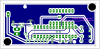
Attached is part of a XILINX CPLD and FGPA programming adapter with the DRC displaying "NO ERRORS".

Just in case somebody is in need of the complete adapter the schematic and layout are packed in the attachment.

Boncuk
 
Last edited:
Sharp Eagle Schematics in OO write

In Eagle schematic editor go to the print dialog and select the PDF box. Instead of printing the schematic it will create a PDF file. Note that over writing a file does not work. Use a new name each time.

Open the PDF file with Adobe Reader.
Do TOOLS>SELECT&ZOOM>SNAPSHOT_TOOL
Drag the select box over the area of the schematic you want to capture.

Place the OO write cursor at the insertion point.
EDIT>PASTE_SPECIAL>BITMAP
The image can be dragged and stretched.
 
Extending the VSS polygon

To make my boards easier to solder I like to use a large isolate value for the VSS polygon. But this can prevent the VSS polygon (aka fill) from getting into some areas.

You can use the WIRE tool to extend the VSS fill through the too-narrow opening and into the region you want filled. Use the NAME tool to change the new wire's name to VSS. Hit RATSNEST and area should fill.

superprobe5_bottom_cheat-png.21204


The pink arrow in the above image points to a wire that causes the area to the left of the arrow to fill.
 

Attachments

  • superprobe5_bottom_cheat.png
    superprobe5_bottom_cheat.png
    55.2 KB · Views: 982
I do a similar thing on thermals connected to high-current pads (e.g., power pads). You can add width or a geometric shape to the connecting bars. Just be sure they are properly named. As far as I know, the width of the connecting bars in thermals cannot be independently changed in V. 4.XX.

John
 
5.2 is out. They have made some improvments to the UI.

The one I like is that if you have move selected and select group, the UI switches back to move after you select the group. Save a few keystrokes.

I like that change too. I'd still like to see automatic grouping though. After working with an editor like LTSpice's, using the Eagle editor is kinda like kicking a dead whale down the beach. I sometimes find myself looking for other ways to do things so I don't have to move groups, which is just wrong. Setting Group to Ctrl-G helps a bit but not much.

Granted, the Eagle editor has to do a lot more than LTSpice's--that was just an example.


Torben
 
Questions

I recall that there is a way to import an image into the library editor to help in laying out parts. If there is there I can not find it.

One thing that bites me from time to time is that I create a symbol that is too large or too small to match the rest of the ones used in my schematic. Does anyone know how to scale them.
 
Hi 3v0,

that happens from time to time if you don't have any possibility of comparison. However in that case just load a symbol of any part to "measure" its dimensions. Thereafter resize the symbol which doesn't match the proportions of other parts.

Hans
 
i have a file eagle file which i need to convert in to a gerber file because the pcb machine my friend has does not recognize brd format but it does have a gerber converter.how can we convert .brd files in to gerber?
 
i have a eagle file which i need to convert in to a gerber file because the pcb machine my friend has does not recognize brd format but it does have a gerber converter.how can we convert .brd files in to gerber?
 
Hi Silvarblade,

from the control panel select Cam Processor. There are two different kinds of Gerber file Cam Processors, one with a number (don't remember the exact number). It is the advanced Gerber processor which is commonly used by PCB manunfacturers.

Before you use the Cam Job, transfer the file to be converted (only the board file) to a separat folder and have the job carried out there. That way you won't have a mix of Gerber files of different projects.

At the end of the process there will be one file with the suffix $$$. You might delete that (the most memory eating file) because it is just a temporary file and of no use for the PCB manufacturer.

Hans

P.S. Must be a poor PCB manufacturer though. Most of them convert all different known board files to Gerber files on their own.
 
Last edited:
hi 3v0, the gerber file format of the pcb machine has gerber extension as .gb and i dont get that format on any of my eagle files. whats the differrence?
 
In the con-subd library. M25
 
thanks mike.one last question i need to make a pcb at home and want to print the board on a bonging paper.the thing it i get image on the whole of the paper and not the original pcb size i-e like a 3x4 etc.how can i do that?
 
Status
Not open for further replies.

New Articles From Microcontroller Tips

Back
Top