earckens
Active Member
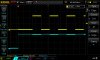
Solved, how stupid can I be: a load to the 555 output with a LED and a p-channel as well to invert the signal.. Except that I had a n-channel installed.. Sorry for that. Now I have a clean square wave again.
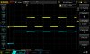
But still having to look as to why the M2 in Wally's schematic does not turn on.. Tomorrow I continue, clearly it gets too late to think non-confused.
But still having to look as to why the M2 in Wally's schematic does not turn on.. Tomorrow I continue, clearly it gets too late to think non-confused.
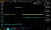
 . However after some time Q8 stops conducting and gets very hot. Then I re-installed a 100k between source and +12V for Q9 and Q8. Still same issue after a short while.