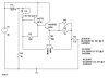
Q: about Darlington Pair.
At first sight, it's an obvious "mechanism."
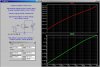
But if you look at a chart for a single (npn) transistor, the current permitted to flow from C to E is a power function of the Voltage applied to B.
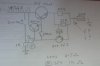
But then that current goes to the base (B2) of the second transistor. The voltage at that point is fixed. So how does the rising current applied to B2 allow amplification of the C2>E2 current? The voltage in the second system is fixed and maximal. So we must be reducing resistance in the base B2, but how does that happen by applying more current to B2??? (of course, I know that current is what matters in reality - but it needs voltage to drive it)
At first sight, it's an obvious "mechanism."
But if you look at a chart for a single (npn) transistor, the current permitted to flow from C to E is a power function of the Voltage applied to B.
But then that current goes to the base (B2) of the second transistor. The voltage at that point is fixed. So how does the rising current applied to B2 allow amplification of the C2>E2 current? The voltage in the second system is fixed and maximal. So we must be reducing resistance in the base B2, but how does that happen by applying more current to B2??? (of course, I know that current is what matters in reality - but it needs voltage to drive it)