Continue to Site

Welcome to our site!

Electro Tech is an online community (with over 170,000 members) who enjoy talking about and building electronic circuits, projects and gadgets. To participate you need to register. Registration is free. Click here to register now.

  • Welcome to our site! Electro Tech is an online community (with over 170,000 members) who enjoy talking about and building electronic circuits, projects and gadgets. To participate you need to register. Registration is free. Click here to register now.

DALI Circuit Explanation

Status
Not open for further replies.

Kisen

Member
Hi,

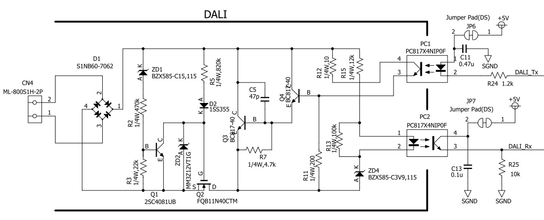
I am looking to use the below circuit in a project i am working on.

For the large part i understand what the circuit is doing, apart from 2 areas. Hoping someone can help.

I am struggling to see what Q1, Q2, D2, ZD2 and R5 are doing.
Also what is the purpose of R13?

Can anyone help me out please.
119822
 
That part of the circuit is a current limiter.

DALI uses a current limited supply where the voltage of the bus (and supply) can be pulled down by any transmit device.

A current limit means the transmitting device can pull the bus voltage down as required without the power source trying to maintain a fixed level and excess current being taken through the transmitter (like a short circuit on a conventional power supply).

According to the DALI standard, the bus power source should be limited to 250mA, though lower currents are sometimes used with short busses and few connected devices.

Edit:
R13 ensures that if there is any leakage current through the zener when the voltage is too low for it to properly conduct, there is not enough voltage across the LED for that to conduct. It also allows the LED to turn off faster when the bus voltage is shorted by a transmitter.

It's good design practice to allow for the fact that real-world components do not always work perfectly, with no leakage.
Like always having a base-emitter or gate-source resistor on a transistor, even if the drive circuits should shut off the current or voltage to the base / gate...
 
Last edited:
Hey, rjenkinsgb.

I was of the assumption that DALI used a current limited power supply and that the power supply itself took care of the current limiting aspect.

As this circuit has current limiting built in does that mean a current limited source is still required or can 16v be applied direct to the bus and this circuit will take care of the current limiting for me?
 
The left-hand part of the circuit, up to R5 - D2 - Q2, appear to be the DALI bus power supply. "There can be only one"...
What is CN4 supposed to connect to, on that unit?


If you are connecting that unit to an existing powered bus, I'd leave out the components after the bridge rectifier through to Q2 etc. and link out the Q2 source and drain connections.


As it's drawn, it looks to really be more a demonstration unit than a fully specified DALI standard unit. I suspect it needs minor mods to be fully DALI compliant.

There is nothing I am aware of in the DALI specs that requires a normal device to contain current limiting.
I can imagine a hypothetical add-on section in a node device to prevent a permanent bus short in case of a device electronics fault, but that would contain a timing network of some sort and the limiter in that design has no time delay, so makes no sense in the context of a node device.

See the Wikipedia article here for some more info:
 
The circuit is taken from this application note.

**broken link removed**

CN4 is the connector to the bus itself. I expect that due to the power supply and current limiting being in this circuit, would it be fair to say that the power supply on the bus is a standard voltage power supply.

Ultimately is this circuit practical (with small changes like base resistors and such)?

I do not specifically need this circuit to be complaint with DALI, I planned to use it more so as a method of communication over long distances where i shall create my own protocol. It looked very appealing due to noise immunity and only having 2 wires.
 
The circuit is taken from this application note.

**broken link removed**
Either I'm going blind or there is no circuit in that document??

This is the schematic for the Renesas evaluation board with DALI and DMX options, which is what the document you link to seems to refer to:
**broken link removed**

The DALI interface is the small section near the top left, from CN2 through to SW1.
 
OK.

That is a strange circuit, I have no idea why they are doing it like that.
 
Status
Not open for further replies.

Latest threads

New Articles From Microcontroller Tips

Back
Top