The circuit consists of stages that are used in the design of a Power amplifier.
input, driver and output stage.
And those stages comprise of sub-circuits
eg. output stage: composite transistors (Darlington & Sziklai types)
driver: VBE multiplier and current source(current mirror, bootstrap circuit)
I'm fully aware of the stages of an amplifier, have designed, built, and repaired many over the years.
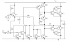
But you can't just randomly throw the pieces together, and the 'circuit' in question is completely wrong in every respect, and doesn't bear any resemblance to an amplifier. The first circuit you posted wasn't quite as bad - at least that was a recognisable design, and just needed correcting. This last one is so far wrong, it wouldn't be correctable - throw it away and start again.
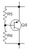
So if I attach a diagram of a sziklai darlington configuration and ask you what it does....your response is going to be
As we've told you repeatedly, that 'circuit' is completely nonsense - it wouldn't work, so they have no effect.
Because its not in a "functional" circuit.
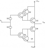
I've no problem with that part of a circuit, but as already mentioned by someone else - it's a non-practical example out of a text book - check the Amplab link I posted earlier that shows the rest of the parts, both of the output stage, and the rest of the amplifier. A Sziklai is just a different kind of darlington.
Here's the actual link to the Sziklai version, note there's 8 pages in the project, showing three different output stage versions:
Sziklai - Complementary Feedback Power Amp Output
But there is so much that can be said about that diagram.
I think you shouldn't reply at all to my thread if you dont want to help.
Forums are an historical record - if we let you post complete rubbish and designs that are wrong in every respect, we're going to get people trying to build them. There are hundreds (if not thousands) of working designs on the net, why not pick one of those?, or at least look at them, and compare them to what you keep posting.