Electro Tech is an online community (with over 170,000 members) who enjoy talking about and building electronic circuits, projects and gadgets. To participate you need to register. Registration is free. Click here to register now.
Welcome to our site! Electro Tech is an online community (with over 170,000 members) who enjoy talking about and building electronic circuits, projects and gadgets. To participate you need to register. Registration is free. Click here to register now.
What exactly do you want to know about it? It looks like a very typical amplifier with a class A-B output stage. It appears to be a schematic of an integrated circuit.
Does it really matter?, the difference between 0.05% and 0.001% isn't very audible
More importantly it's not a real design, various bits are missing (such as emitter resistors, feedback decoupling capacitor, input coupling capacitor), and many of the values are completely wrong.
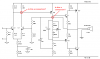
Rin≈R17;
Voltage gain≈(1+R9/R10)
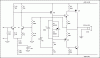
Q1, Q2 is a input differential stage.
Q8 is a main voltage amplifier stage with bootstrap load C2, R3 , R4.
Output stage is a complementary feedback pair ( Sziklai output).
Q4 vbe multiplier provides AB biasing and prevents from thermal runaway.
If Q4 is thermal coupled with Q4.
Everything is there to build it. A good electronics wiz could easily reverse engineer the circuits to get the nessisary calculated range of allowable tolerances for the transistor component values and should be able to pick what fits the aplication from that. It might not be high quality or high performance but its doable.
The writing looks just fine on my 30 inch LCD monitors.
Distinguishing what the different stages in the circuit are. What the stages do. What components make up the various stages. Flaws, improvements & errors in the circuit. Even raising questions on power amplifiers based on the given circuit. I want to swamp myself with thoughts of power amplifiers, i want to get a feel for it when I see circuits. Any useful comments on the circuit will be appreciated. Thanks to all that are contributing
Thanks Hero999. The circuit looks much better now.
More importantly it's not a real design, various bits are missing (such as emitter resistors, feedback decoupling capacitor, input coupling capacitor), and many of the values are completely wrong.
It needs throwing away and starting from scratch - there's a free guitar amp book on the foum, I would suggest you try downloading that and having a read.
That's because it's not an English diagram, the Dutch magazine Elektor uses E instead of R (although they would never publish such a poor non-working circuit).
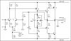
Circuit 2 (in the attached diagram) is a standard circuit with single Vcc and complementary o/p stage as opposed to
Circuit 1 which was configured with Sziklai o/p and dual supply.....
This site uses cookies to help personalise content, tailor your experience and to keep you logged in if you register.
By continuing to use this site, you are consenting to our use of cookies.