Continue to Site

Welcome to our site!

Electro Tech is an online community (with over 170,000 members) who enjoy talking about and building electronic circuits, projects and gadgets. To participate you need to register. Registration is free. Click here to register now.

  • Welcome to our site! Electro Tech is an online community (with over 170,000 members) who enjoy talking about and building electronic circuits, projects and gadgets. To participate you need to register. Registration is free. Click here to register now.

Thermal pads in Eagle

Status
Not open for further replies.

sfink06

New Member
Hi all,
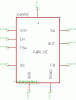
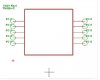
I have a circuit in eagle that contains a TPS61081 IC. The IC includes an "exposed" thermal pad. I want to connect this thermal pad to the ground plane using a thermal via. The problem is, while the board does show connections for thermal pad, there is no way that I can see on the schematic to connect the pad, and I do not know how to add a via manually on the board. I have tried to use the invoke command, but I get an error that says: "The part had only one gate: U$1."
 
Hi,

the problem with Eagle is the fact, that it won't allow to create SMD pads other than rectangular.

In that particular case you would have to use five SMD pads, one 2.4X1.65mm, and four pieces of 0.75X0.23mm, placing them according to the datasheet outline. I'd call them TP1 through 5.

The symbol must contain those 5 pins as well to create a proper device. I suggest to put them underneath the "frame" of the IC-symbol. (pin length - point, visible - off)

The symbol should look about like this: (attachment) Note that one of them is loacated just on top of the regular ground pin. So you just need to extend the net into that pad.

Save the symbol and create a device using that symbol and the package you have already done.

Connect pins and pads as you do with any device.

That method has the advantage, that the solder stop will include the entire thermal pad.

Boncuk
 

Attachments

  • TPS61081-SYMBOL.gif
    TPS61081-SYMBOL.gif
    6 KB · Views: 952
  • THERMAL-PAD.gif
    THERMAL-PAD.gif
    5.3 KB · Views: 1,222
Last edited:
okay, here is what the schematic symbol and board symbol look like right now. As you can see, the board symbol shows the rectangular pads for the thermal pad, but there are no pins on the schematic that correspond. Do they need to be manually connected from the board with the thermal via, or should there be connections made on the schematic? :confused:
 

Attachments

  • sch.JPG
    sch.JPG
    21.5 KB · Views: 642
  • smd.JPG
    smd.JPG
    16.6 KB · Views: 693
You definitely used the wrong layer when designing the thermal pad. You must use the top layer and SMD pads to do it. Also, your symbol doesn't contain any pins to connect to the thermal pads.

The four "fins" are not supposed to produde over the IC-body.

That will neither work in the schematic nor in the PCB layout. If you want to use the IC mounted on the solder side you place it on the component side first and then mirror it. All SMD pads will turn from red to blue indicating that the IC is bottom mounted.

I guess I described the procedure clearly enough.

You might choose an easier way making one rectangular pad only for "TG" (Thermal Ground) and draw the small fins using the top layer. They won't be connected to ground (since they are no pads) but be connected automatically to the center pad if they are drawn without gap adjacent to that.

Warning:

In that case you won't be able to mirror the device, since the rectangular "fins" are no pads and will remain on the component side stealing valuable space for routing. (They won't be part of the device)

Once again: Your symbol must contain at least one pin for the thermal pad. If it's name is also "TG" you connect the pin to the pad with the same name when creating the device.

Boncuk
 
Last edited:
Status
Not open for further replies.

Latest threads

New Articles From Microcontroller Tips

Back
Top