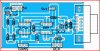
Continue to Site

Welcome to our site!

Electro Tech is an online community (with over 170,000 members) who enjoy talking about and building electronic circuits, projects and gadgets. To participate you need to register. Registration is free. Click here to register now.

  • Welcome to our site! Electro Tech is an online community (with over 170,000 members) who enjoy talking about and building electronic circuits, projects and gadgets. To participate you need to register. Registration is free. Click here to register now.

Struggling to do my own ELectronic Stuff?

Status
Not open for further replies.
On further thought of what you are doing or trying to do i am a little confused about the motor operation


Now what turns the knob on in the first place?

Is the motor turning the knob on and off?
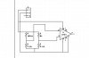
If so, then there is a need to forward and reverse drive the motor, which will need a relay or H bridge of some description to reverse the polarity to the motor.

If all the circuit is to do, is turn the Knob off in the absent of a flame, then the circuit will work as designed, but how do you turn the Knob on with a motor attached to it.

It would be much easier to use a solenoid to switch the gas flow on/off prior to the knob.
Although a solenoid would not be good to run from batteries.

Pete.

First of all thanks for your reply!

Now with regards to the nob. The motor will only turn the nob OFF. It's for my gas cooker so I am going to turn the nob ON and OFF. If at some point the gas is leaking and the nob is ON then the motor will turn on, turning the nob OFF.

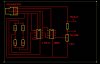
Also, I can see that I could drop the Op-amp and just use an ADC, connecting the thermistor directly to the PIC, but I am actually just playing around with this circuit and want to learn to use OP-AMPS as well. So at this point I would rather keep it in the design as I made it (but replacing it with a comparator instead of my 741). Of course after I make the circuit and it works etc I will change it and then maybe use an ADC instead.

I like to keep things simple by using stuff I am familiar with and then moving on, instead of changing stuff half-way through (or do you think that's a bad approach?)

Also I hope my code wasn't confusing was it? I thought it was neat! (but then again, im not very good at coding so I guess I just have to learn to be neater)

Thanks!

Fouad.
 
Last edited:
Something SABorne mentioned that would be a very good idea is to use the solenoid as a gas valve. I wasn't sure what the motor deal was about. I realize you are just messing around with this, and it makes for a great topic, but remember if any of this becomes real be careful working with gas as in real life there are considerations. Mean time, have at it. :)

Ron

Thanks, I will make sure anything I do, I do it safely! But I must say, I really dont know what to do with this error that I keep getting on the PCB Software (I'm using Proteus 7, ARES). I described it on post #9.
 
I like to keep things simple by using stuff I am familiar with and then moving on, instead of changing stuff half-way through (or do you think that's a bad approach?)

Also I hope my code wasn't confusing was it?

Its your circuit and you are free to build it as you see fit, i find doing things in software much more flexable and a reduced component count makes producing a PCB much easier.

As for your code.......Hmm to be polite...its a mess.
The up side was at least you had a go and are learning, so i can only expect it to get better.
I spend a reasonable amount of time on the Picaxe forum too, and dont know of anyone else who writes code like you do all strung togther.

Some of my projects have over 1000 lines of code and if i wrote it like you do, i would never have a clue of what the heck it was doing.

I have never used Proteus so i am unable to help there.
I use ExpressPCB as it is dead simple to use, and i can draw a small layout manually rather quick.

Pete.

OO I just downloaded ExpressPCB and it seems quite good and simple. Guess I'll just play around with it and learn how to use it properly. Then I can use that for my projects instead of ARES.

I guess I will be asking for help a LOT from you SABorn lol (hope you don't mind)

Fouad.
 
I am now trying to use the ExpressPCB software. How do I know which type of PIC to add to my schematic for it to work with my own project. I am sure it has to be a DIP8, but not sure which one...

I have attached what I have done so far in this post.

Thanks.
 

Attachments

  • circuit.jpg
    circuit.jpg
    47.1 KB · Views: 136
I often dont use a pic from the library and just draw a rectangle using the square tool to the left hand side, than add the legs as needed, as i did for the earlier schematic i done for you.

You could use the Microchip pic 12F675 footprint, for the 08m.

You dont need to do a schematic to produce the PCB design and can just draw the pcb as needed.

If you have a go at the pcb and post the artwork file i will have a look and tidy it up for you if it is needed.

Try to keep your tracks and pads as large as practial, as this helps when you start out to make boards, and you dont get as many errors with etching etc.
I have a view of, why remove the copper if you dont need to.

We are all here to help and share advice, to those who are prepared to listen and learn.

A year or two ago i put together this article about making PCB's you might like a look at.

https://www.thebackshed.com/windmill/articles/MakingPrintedCircuitBoards.asp

Pete.
 
Last edited:
I often dont use a pic from the library and just draw a rectangle using the square tool to the left hand side, than add the legs as needed, as i did for the earlier schematic i done for you.

You could use the Microchip pic 12F675 footprint, for the 08m.

You dont need to do a schematic to produce the PCB design and can just draw the pcb as needed.

If you have a go at the pcb and post the artwork file i will have a look and tidy it up for you if it is needed.

Try to keep your tracks and pads as large as practial, as this helps when you start out to make boards, and you dont get as many errors with etching etc.
I have a view of, why remove the copper if you dont need to.

We are all here to help and share advice, to those who are prepared to listen and learn.

A year or two ago i put together this article about making PCB's you might like a look at.

https://www.thebackshed.com/windmill/articles/MakingPrintedCircuitBoards.asp

Pete.

YOUR AMAZING!

Thanks!

I shall try just to draw the PCB and as you said. I will send it to you when I finish! (also do you mind telling me what things your fixing and why after changing it?)
 
Yes i will tell you what i change if it is needed.

I find in Express the pad sizes in the libaray have large holes in them and this makes drilling hard, so i create my own using 2.11mm outside diameter and 0.51mm hole size, as this is as big as i can go for between pins etc.

I very rarely ever use the component footprints as they also have big holes so just use my custom pads and tracks to design a board, it gets rather quick once you do a few designs.

I dont need to check your work unless you want me to, that is up to you to decide.
I dont think you can post a express file to the forum, so you might need to email it to me, i think my email is active on the forum, if not Pm me and i will give a email address.

Pete.
 
By the way, what do you call these connectors that you connect VCC ,GND and Pin 3 of the 08M to? (as shown in my circuit diagram). I cant find any from Rapid...
 
Ok, I have now made the first draft of the PCB. I want it all to be on one side, so it's connections are a little long winded (and I don't have a lot of intuition of how to make it simple yet). I still don't know how to buy the connector, so I just added one that looked okay.

I didn't find a lot of space to label the gnd/VCC connections on the connector, but it's not hard to figure out which is which.

SABorn did talk about making my own footprints, but seems a bit tedious and I probably want my holes a little big so I have some margin for error when I drill :)

Anyway, do give hints/tips as to what I could improve and I shall try my best.

The Components I will use are found here:

Diode: **broken link removed**

MOSFET: **broken link removed**

OP-AMP (LM311): **broken link removed**
 

Attachments

  • PCB-noconnector.jpg
    PCB-noconnector.jpg
    142.5 KB · Views: 135
Last edited:
The connectors i think you have used are 2.54mm pitch header connectors, i use them a lot and the pin spacings are the same as a IC is 2.54mm apart.

Look here.
**broken link removed**.

I often use the 3 pin ones as a programming socket for the picaxe and have an adapter lead made up to go from the serial D9 socket to the header plug.

With the holes a small hole in the copper pad from etching makes it easier to drill, as the drill bit will locate centre of the pad, where a big hole in the copper allows the bit to walk around in the copper hole and often drills off centre or breaks the bits.

Big pads and small holes are the way to go.
Big holes drilled in the board makes soldering much harder as the solder needs to bridge the gap from copper to component leg.

The diode you choose is a bit light for the job i would think and be better to use a power diode like a 1n4001 or 1n4007.

Pete.

Ah, ok.

I will buy the connectors you gave me!
Now I shall make the Pads big and the holes smaller and make sure I order the 1n4001or 1n4007 diodes.

Does the rest seem okay though?

Thanks.

...I dont know how to make my pads bigger and my holes smaller lol

Do you mind showing me how to do that?
 
Last edited:
Select a pad in Express from the LH tool bar, then in the top RH corner you have "Create new pad" (gee wonder what that is for) select it and you will get a box pop up to design a pad in.
Select a shape from the drop down menu
Select a hole size from the drop down menu, ...use 0.51mm the smallest hole on the list
Then select the outer size of the pad size, type in 2.11mm as this will be as big as you can go and not get errors between pins. click OK.
Now the new pad will be in the menu of pad sizes to pick from.
If you click the drop down menu just to the left of the Create a new pad box in the top tool bar.

Pete
 

Attachments

  • express.JPG
    express.JPG
    63.5 KB · Views: 130
Thanks!

Ok, I have now made the pad. Though does this mean I have to create custom components since I can't just put the pad on top of each component can I?

I can't seem to edit the pads in the existing components either...
 
I can't seem to edit the pads in the existing components either...

You can edit them, what you need to do is place the component on the screen then click on the component to highlight it, then go to "EDIT" in the top tool bar and click "UNGROUP" now you can draw a rectangle around the pads and double click on a pad it will allow you to change the pads, once changed, draw a rectangle around the whole component and go to EDIT again and click "GROUP" now the footprint will be locked back together again.

If i need the footprint again i just copy paste it as many times as i need.

The Group and UNGROUP also works in the schematic program should you need to change a component in there too.

The free version of express wont let you save custom components to the file, so what i do is create them and leave them off to one side of my circuit, and copy paste them into the circuit, this way you have your own common used footprints and when i go to a new circuit design i just copy the lot of the home made footprints from the previous circuit and paste them on the page of the new circuit, then work from there, i also find this much quicker than looking for a component in a long list of stuff i dont want.

Lets face it what do you often need, resistors, diodes, 8,14,16,18,20 pin IC, a few capacitors, is the bulk of what you use frequently, the rest i just make as needed, or use plain pads.

The more you do the quicker it gets.

Pete.


Sorry it took me so long to respond! I have now changed all the pads and attached a picture to this post.

Anything else I should worry about before trying to make it?

Thanks!
 

Attachments

  • CircuitChanged.jpg
    CircuitChanged.jpg
    149.9 KB · Views: 115
Anything else I should worry about before trying to make it?


Yes there is.

Your track size is way to small, and need to be increased to 1.02mm to 2.03mm range.

This might look rather big on the screen but will produce a nice board, as i keep telling everyone when you make a board leave as much copper on the board as you can, if it dont need to be removed than dont remove it.

I frequently use 2.03mm tracks as it makes for strong pads with big tracks, and you have the space on the board to do this.

It also helps to prevent problems you might encounter when you go to etch the board.

Here is an example board i done of your circuit a week ago, to give you an indication of what i mean by big tracks and leaving as much copper on the board as i can.

I used a fill plane around the board to fill in the blank spaces but you dont need to do that if you dont want to. (it can be a little tricky to start with)

The less copper you etch away the faster the board will etch and the longer your etch solution will last.

Pete.
 

Attachments

  • Example board.JPG
    Example board.JPG
    59.3 KB · Views: 157
Next problem..........

You dont have the programming circuit for the 08m on the board, (10K and 22K resistors) so how do you intend to program the chip???

Also it is very important to have the programming circuit (2 resistors) in circuit at ALL times with the picaxe or you will get problems with the operation of the picaxe, it must be included on the PCB, even if you dont use it.

You should also add decoupling capacitors to the circuit, this means 0.1uf cap as close to the picaxe as able between 5v and ground.

It would not hurt to add some further filtering to the board like a 10uf cap as well because you could get some noise from the motor feeding back into the power rails.

Problem #3.

I just realized you have designed the board on the top layer of the board and for a single sided board it needs to be designed on the BOTTOM layer.
No big problem......Draw a rectangle around the whole board to highlight it all, then go to EDIT and click SEND TO BOTTOM LAYER, then click save.

It should now be in the green yuck colour. (i changed my colour to blue) Green is the bottom layer, red is the top layer.

When you go to print and dont select colour print, it will print the image in reverse as you need it to be.

Pete.
 
Last edited:
Status
Not open for further replies.

Latest threads

New Articles From Microcontroller Tips

Back
Top