Greetings,
I am working on a flyback smps.
Currently I am having a problem with the mosfet switching, the mosfet itself won't mirror the drive
signal from the PWM controller, only a distorted pulse appear. I am sure the PWM controller is able
to drive the mosfet without a problem as the input capacitance of the mosfet is max. 750 pF and
the allowed capacitance for the PWM controller is 1 nF.
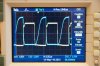
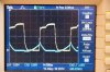
I guess the "distorted" wave at 0 V AC doesn't tell much, but check the huge spike over the transistor @10 V AC, it's like 50 V, shouldn't be so high, it looks like the transistor is operating wrong and the spike from the 0 V screen gets amplified.
The voltage between drain and source shouldn't be higher than 10 V * sqrt(2) (+ possible spikes).
I've tried several transistors now, still this strange issue, the GS voltage and everything seems to be correct...
Input from mains: 230~ V AC -> 325~ DC
Switching frequency: 450 KHz
output voltage: 19 V
output current max.: 4.74 A
parts:
PWM controller: UC3842
Mosfet: 2SK2700
The PWM controller receives power from an external power supply.
Circuit schematic and signal captures from the circuit are attached.
In the signal captures the yellow line is the switching from the PWM controller, blue line is the drain-source voltage @ 0 V AC and 10 V AC
Any pointers are welcome


I am working on a flyback smps.
Currently I am having a problem with the mosfet switching, the mosfet itself won't mirror the drive
signal from the PWM controller, only a distorted pulse appear. I am sure the PWM controller is able
to drive the mosfet without a problem as the input capacitance of the mosfet is max. 750 pF and
the allowed capacitance for the PWM controller is 1 nF.
I guess the "distorted" wave at 0 V AC doesn't tell much, but check the huge spike over the transistor @10 V AC, it's like 50 V, shouldn't be so high, it looks like the transistor is operating wrong and the spike from the 0 V screen gets amplified.
The voltage between drain and source shouldn't be higher than 10 V * sqrt(2) (+ possible spikes).
I've tried several transistors now, still this strange issue, the GS voltage and everything seems to be correct...
Input from mains: 230~ V AC -> 325~ DC
Switching frequency: 450 KHz
output voltage: 19 V
output current max.: 4.74 A
parts:
PWM controller: UC3842
Mosfet: 2SK2700
The PWM controller receives power from an external power supply.
Circuit schematic and signal captures from the circuit are attached.
In the signal captures the yellow line is the switching from the PWM controller, blue line is the drain-source voltage @ 0 V AC and 10 V AC
Any pointers are welcome
")