still wont work well
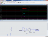
https://cscott.net/Projects/FabClass/final/Schematic/edm-power.pdf
read ,, understand then ask questions
https://cscott.net/Projects/FabClass/final/edesign1.html
misc
https://cscott.net/Projects/FabClass/final/Schematic/saviers-email.html
set pulse width, say 50 to 200 us and pulse interval, say 200 us to 2 ms.
Ultra Low ESR Caps are critical for best performance
e.g. not including MOSFET RdsOn
$13 10000µF * 33 mΩ = 330 us " "
$16 10000µF * 18 mΩ = 180 us, " "
$32 10000µF * 8 mΩ = 80 us " "
$37 10000µF * 7 mΩ = 70 us " "
If it just states Ripple current ignore that part.
Last edited:


 Do you think he can share one charge pump with the 2 IGBTs?
") . Wife and I are going to classes for home dialysis for her and it is mind numbing. Am working on a better schematic showing what is needed. Thanks for the comments and help.
. Wife and I are going to classes for home dialysis for her and it is mind numbing. Am working on a better schematic showing what is needed. Thanks for the comments and help.