Continue to Site

Welcome to our site!

Electro Tech is an online community (with over 170,000 members) who enjoy talking about and building electronic circuits, projects and gadgets. To participate you need to register. Registration is free. Click here to register now.

  • Welcome to our site! Electro Tech is an online community (with over 170,000 members) who enjoy talking about and building electronic circuits, projects and gadgets. To participate you need to register. Registration is free. Click here to register now.

Pulsar Stuff

Status
Not open for further replies.
Yes, I agree, although I didn't bother mentioning it because of all the grief I got last time.

Here's how I like to do it.
 

Attachments

  • Noise gen PCB T jun.png
    Noise gen PCB T jun.png
    68.2 KB · Views: 154
great looking board for first one

definitely do a filled plane with wide clearances between planes and traces.
be sure to burnish the edges of the board to avoid any high spots.
print out in a high density like 5 on an HP 1320 laser printer.
I perfer the 1 part murtic acid to 2 parts hydrogen peroxide (ADD the hydrogen peroxide TO the acid) in a plastic container. The Pulsar site mentions using a plastic bag.
run the boards through the lamina tor in opposite directions several times like 3 - 5 x's
CLEAN the boards ( I perfer a drop of dish soap and green scotch brite pad. A 600 wet dry paper works good to.
do not get finger prints on the board surface.
allow about 5mm clearance around the perimeter of your board design and traces Traces should be for a 1st board .25-.30 inches wide.
don't forget to mirror the bottom design.
depending on how heavy your copper boards are (the ones in the kit are 1/2 oz I believe, the etching will take 2 - 5 minutes and the etchant will turn green
use the green foil after you have applied the toner transfer.
cool the board immeditaly after using the lamina tor at eac step.
when all done then I like using liquid tin to prevent corrosion and it seems to aid in soldering.
If you need any help then call PULSAR. Great support.
I know a lot of this is repeated but it all is important to know
most important - let us knopw and see your results
 
I think you know this already, but your text is on the top layer. If you want it to etch with your board and be readable, you need it to be on the bottom layer. Just use the mirror tool.

Since you are using the bottom layer (blue), you don't need to print mirrored. The bottom layer is already mirrored, so just print it as is. If you use the top layer, then you'll have to mirror when printing.

You can remove the top jumper all together just by moving the trace you are 'jumping' over around the thru-hole to the left.
 
Free DIY toner transfer paper trial.

whats a fillet?

With out seeing the component parts of your design I can only guess how many parts there are.
Using a comparator you can get the parts to 9ea.

If you are in no hurry I can replicate your board in ExpressPCB, print two copies and let you try it.
No laminator required.
I will also let you try my DIY toner transfer paper.
Or to make it easier I can mail you a sheet of it to try. It has a money back guaranty! :)

I have got little feedback on on the subject thread and it seems to have died.

Anyone else?
 
G'day Jason,
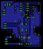
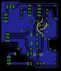
That second design does look a heap better mate, now what I do with my designs where a T or junction come off a track I put a fillet in each corner so the junction is alot thicker. If you add that then hero999 might not wet his nappies as after some of his replies to other peoples boards really makes one wonder if indeed he did wet himself.

Cheers Bryan :D

The fillet idea is great, have been wondering about how to make that look neat.

Thanks.
 
Rolf sure you can mail me a sheet. If its free :D

I will fillet the parts now. Also i hate ground planes. Maybe because i dont know how to do them well :D
 
Rolf sure you can mail me a sheet. If its free :D

I will fillet the parts now. Also i hate ground planes. Maybe because i dont know how to do them well :D

You use EAGLE don't you Jason? Then it is easy. Just select the polygon tool and draw a rectangle around your board on the layer you want the fill on. When you have done this select the name tool and click the polygon you just created and name it gnd. The polygon will fill in and give you a ground fill. I use the design rules to increase the clearance when etching my own boards so they are easier to solder.

A ground plane is a separate layer which is only ground - if you want to get technical.:p
 
Rolf sure you can mail me a sheet. If its free :D

I will fillet the parts now. Also i hate ground planes. Maybe because i dont know how to do them well :D

Drop me a Private Message with your address. It is free.
 
Last edited:
I must be the only person here who runs tracks direct (ie at any angle) to keep current paths as perfect as possible. Yeah I know American electrons can only travel at 45' and 90' (it's in the RULES man) but here down-under our Aussie electrons are more laid back... they seem to prefer shorter more direct tracks... ;)

Abolish cruelty to electrons! :D
 
LOL Mr RB....

Hey guys How do i change the rules on the ground plane? Like how it seems too close too me. How do i set the distance between the trace and the gnd?
 
LOL Mr RB....

Hey guys How do i change the rules on the ground plane? Like how it seems too close too me. How do i set the distance between the trace and the gnd?

Yea, Roman should change location from 'out there' to 'way out there' :p


to change the rules go EDIT -> DESIGN RULES... choose the tab CLEARANCE then adjust the space between track to track (WIRE)
or track to pad (WIRE & PAD) or pad to pad (PAD & PAD) .... etc.

EDIT: the change may not show up until you hit RATSNEST again

From the design rules:
EAGLE Design Rules
The default Design Rules have been set to cover a wide range of applications. Your particular design may have different requirements, so please make the necessary adjustments and save your customized design rules under a new name.

You do know about the ULP 'drill-aid,' don't you?
 
Last edited:
nope whats that?

Thought you may not, so I left EAGLE running lol :p

From the FILE menu choose RUN... then navigate to a directory in the installation called ULP and choose 'drill-aid.'
I have a button on the toolbar - you may too...

It will make all of your drill holes very small, just enough to start the bit in the hole... very handy (thanks to 3v0 for this tip!)

it does this on a different layer in case you have to remove them later...
 
Jason,
Possibly the device which fits the three holes on the lower right as I view the board could be 'flipped around' so its ground connection would be on the same side as your ground fill. This would eliminate the need for a jumper there, and would change the layout, perhaps...

What I do is close the schematic file, then rename the board file (add a number to the end or something) then close it. The next time you open the schematic you can create another board with the 'switch to board' command. This allows me to play around with my designs... and see which I like best.

BTW, your board looks much better than the first one.:)
 
You can remove the top jumper all together just by moving the trace you are 'jumping' over around the thru-hole to the left.

See attached with yellow redraw.

You can increase the space between the ground plane and the surrounding traces/pads by increasing the 'isolate' value when you create the polygon. ..or use the 'i'nfo button on the surrounding polygon line and you can change all it's attributes after the fact.
 

Attachments

  • jumper.jpg
    jumper.jpg
    73.8 KB · Views: 129
thanks! and i hope it works well :D

This morning I made a side by side comparison, both transfered at the same time, between a magazine paper and my Elmer's treated paper.
Elmer's treated paper slid off after a few minutes in hot water and you all know what I takes to get the magazine paper off. Note, that the hot water helped even the removal of the magazine paper tremendously.
I don't think it is too shabby:
 

Attachments

  • CIMG3552 s Mag - Elmers PCB comp.jpg
    CIMG3552 s Mag - Elmers PCB comp.jpg
    496.6 KB · Views: 161
Status
Not open for further replies.

New Articles From Microcontroller Tips

Back
Top