Continue to Site

Welcome to our site!

Electro Tech is an online community (with over 170,000 members) who enjoy talking about and building electronic circuits, projects and gadgets. To participate you need to register. Registration is free. Click here to register now.

  • Welcome to our site! Electro Tech is an online community (with over 170,000 members) who enjoy talking about and building electronic circuits, projects and gadgets. To participate you need to register. Registration is free. Click here to register now.

Parallel port driving ADC problems..

Status
Not open for further replies.
Hi Eric,
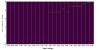
Thanks for sticking with it, much appreciated!:D Your programs confirm the readings I'm getting, for an input of 0V the readings are clearly around this value, the same for an input of 5V. For each voltage input the results are actually not totally random but form part of a set of values. I did some graphing of the readings as you suggested and some interesting results were thrown up. I've combined the results into a single graph ( see attached ). For each voltage input ranging from 0V to 5V in steps of 0.25V, I took 100 readings and plotted them on their own graph along the x-axis. There is some sort of transition around an input of 2.5V. I don't know what these results are an indication of. I've searched the internet for example circuits utilising the 2543 and it seems to be a popular IC for ADC conversion, but I haven't as yet come across any mention of this particular problem. There are suggestions as to how to wire the 2543 up in terms of seperate grounding of the analogue, digital and power supplies in order to minimise errors, but I gather that this is to ensure full potential accuracy as opposed to overcoming seriously bad readings. I'm going to re-arrange the grounding and see if this makes any difference...

Thanks,
Salvatore.
 

Attachments

  • Graphs.jpg
    Graphs.jpg
    218.2 KB · Views: 183
hi salvatore,
Looking at your drawing, you have not shown a 0V gnd connection from the parallel port Pin18 thru 25, to the external power 0V gnd line???

Is this a dwg error?
 
Hi Eric,
Yes, that is an error or rather an omission, I have pin 25 as the ground. I've done some further analysis. I've used the DAC to supply a range of input voltages to the ADC from 0V to 5V in steps of 20mV. For each voltage input I took 100 sample readings and averaged them. I plotted these average readings on a graph, with input voltages along the x-axis and averaged ADC readings along the y-axis ( see attached graph ). The results are very consistent from run to run. I've changed the grounding but the result are the same.

Salvatore.
 

Attachments

  • Graph2.jpg
    Graph2.jpg
    114.5 KB · Views: 160
Hi Salvatore,
Have looked thru your results graph.

Is it possible that you could post a copy of your latest program?

On your original program in the first address sequence, where you had the copy/paste error, are you still switching Dta2 CS line, on the D9 clock cycle??
If so, you are resetting the ADC's internal counters and all your sampling will be out of sequence. This could account for the 'repeatable error' in the results.
Regards
Eric
 
Hi Eric,
I've attached some files that contitute the source code and the installation package. I had to do a major tidy up on the code as it was starting to get messy with all the quick and dirty test code that was added..! :D I had to split the installation package into 5 pieces as I couldn't upload in a single .zip file ( the upload size for a .zip says 9.54MB but anything over 1MB fails..? ). Unzip all the Package files into one folder ( discard the .txt files ). Run setup.exe to install the program, controls, etc. You should then be able to view the source code in full. Let me know if you have any problems..! :)

Thanks,
Salvatore.
 

Attachments

  • Source.zip
    11.5 KB · Views: 126
  • Package1.zip
    66.6 KB · Views: 132
  • Package2.zip
    563.6 KB · Views: 123
  • Package3.zip
    706 KB · Views: 122
  • Package4.zip
    707.1 KB · Views: 149
  • Package5.zip
    429.3 KB · Views: 124
hi,
Downloaded the zips, unpacked OK.
Program runs as *.exe and in VB design time OK.

Using the 4013 test jig, the ADC results are correct???

I will do more work on the program tomorrow.

Regards
 
Hi Eric,
Guess what? I found out what the problem was... the DB25 printer cable I was using..! Doh! In order to test if the software worked on another machine, I downloaded the software to a laptop, connected the printer cable as normal and I got exactly the same rubbish results. But because I could get the laptop very close to the circuit I decided to remove the cable and plugged the circuit's DB25 male connecter straight onto the laptops parallel port, and hey presto, a straight line graph..! :D Analysing individual ADC reads, the 5 LSB's are a tad random meaning a 32/4096=0.0078% error at full scale. This is still pretty good for my purposes but I know the ADC is capable of better. This is more than likely the inputs and/or the way the circuit is laid out so a bit of work to do there. This also begs the question about the cable itself. Clearly it is only the DATAOUT line that is getting corrupted because the other lines are working well enough to drive the DAC with no problems. As an experiment I'm going to change the DATAOUT line for use with another status pin and see what result I get. It may be that he cable itself is at fault I'll have to see. Any how, after all that banging my head against a brick wall the mystery is finally solved..phew..! Thanks for all of your help, it certainly kept me going! :D

Thanks,
Salvatore.
 
Hi Salvatore,
Pleased to hear you are making good progress.

I have found that the 'makeup' of parallel cables can vary quiet a lot.
Some have a data wire twisted with a dedicated 0V wire, others rely on a overall outer screening, some dont have all the 0V's, pins 18 thru 25 connected.

Also the length of the para cable should be as short as possibe, the pulse edges become degraded, some homemade para programmers can suffer from this problem. It is possible to fit non-inverting buffers on the data lines if its necessary to have a longer cable.

Regards
Eric
 
Hi Eric,
I replaced the parallel cable with one of the same length made up from cat5 network cable. Even though the network cable has 10 times less resistance the data on the DATAOUT line is still getting corrupted. I think this is because the signal from the ADC is too weak to send down any significant length of cable. I think I'm going to have to use a buffer of some sort. I was thinking of the 4050B or would a darlington array be better suited?

Thanks,
Salvatore.
 
saiello said:
Hi Eric,
I replaced the parallel cable with one of the same length made up from cat5 network cable. Even though the network cable has 10 times less resistance the data on the DATAOUT line is still getting corrupted. I think this is because the signal from the ADC is too weak to send down any significant length of cable. I think I'm going to have to use a buffer of some sort. I was thinking of the 4050B or would a darlington array be better suited?

Thanks,
Salvatore.

hi,
I would use a HEF4050 non invert buffer, rather than the darlington array .
Its possible that the ADC is unable to drive the ports TTL input directly, as its also got a pullup resistor to +5V.

I use a AD7705 dual 16bit ADC thru the port without problems, but I will have a closer scope view of the ADC Dout signal.
Have you a good cro/scope, so that you could examine the Pin#10 signal?

Regards
Eric
 
Last edited:
Hi Eric,
I have an old beast of an oscilloscope, a large and heavy valve operated tectronix that had served me well, I think remember seeing something very similar in one of the older James Bond films..;) . Unfortunatley I think one or more of the valves have gone ( determined by not being able to see as many glowing points of light as before as viewed through the back of the grill ) which means the 'dot' on the screen is now just a fuzzy blob..shame.. :( .
As an experiment I placed a transistor (2N7000) with a pull-up resistor on the DATAOUT of the ADC and used this to drive the signal down the cable. It inverted the data bits but it worked fine and I was able to use the original parallel cable, so this confirms use of a buffer of some sort for all of the inputs/outputs. You say that a hex buffer would be preferable over the Darlington, I would have thought the Darlington would give the best chance of driving the signal down the cable? Ideally I need a package that will accept TTL/CMOS inputs as well as provide TTL/CMOS outputs, will the 4050 do the job?

Thanks again,
Salvatore.
 
hi Salvatore,
As the ADC is a CMOS device I would use the HEF4050 on the Dout line, its designed to accept CMOS inputs and drive 2 * TTL inputs [fan out]
Refer attachment.

If you would like to study alternatives look at the HCT device range of ic's.

I am currently trying a HEF4050 on my parport project board, it works fine.

Regards
Eric
 
Last edited:
Hi Eric,
Looks like the 4050 will do the job for the ADC DATAOUT, and correct me if I'm wrong, although not specified as TTL to CMOS, according the datasheet it looks like it'll do the reverse and accept TTL levels from the parallel port and output CMOS levels for the ADC. If not, do you know of any 'all-in-one' packages that will accept TTL/CMOS inputs and also be able to drive TTL/CMOS?

Salvatore.
 
Hi Eric,
Had a closer look at the 4050 and I'm not sure that it will be safe with a TTL input as the high level input voltage is specified at V2.75. Although my PC's parallel port seems to output a + 4V 'HI' I can't be sure this will be the case on another machine. I found this though: 74HCT241/244 ( see attached datasheet ). Looks like it's designed to do the job both ways in one octal package, what do you think?

Salvatore.
 

Attachments

  • 74HCT241.pdf
    38.4 KB · Views: 186
saiello said:
Hi Eric,
Had a closer look at the 4050 and I'm not sure that it will be safe with a TTL input as the high level input voltage is specified at V2.75. Although my PC's parallel port seems to output a + 4V 'HI' I can't be sure this will be the case on another machine. I found this though: 74HCT241/244 ( see attached datasheet ). Looks like it's designed to do the job both ways in one octal package, what do you think?

Salvatore.

Hi Salvatore,
I have completed the test of the HEF4050 bfr on the parport with the AD7055 the edges are cleaner/faster.
I would not expect the signal/lines on the parport to much more than +4V, when high.

If you are designing a commercial product and the build budget can absorb the cost of the 74HCT,
it would be wise to try the 74HCT24X.

If you want to keep it simple, using the 2N7000 on the Data line, have a look at pin #11, its inverted within the PC's parport.

For ref, a link. www.interfacebus.com/voltage_threshold.html
Click on the 'voltage translation' link shown in the text

Regards
Eric
 
Last edited:
Hi Eric,
This is purely a personal project, no commercial intent..! Thanks for doing the analysis on the 4050! I'm in two minds as to whether to use a buffer, it would be handy to be a able to utitlise the spare data and status lines for extra input/output switches, but it also depends on how it will perform when sending the signal down a 2 meter length of parallel port cable. The 2N7000 on the inverted status pin is attractive as it is simple ( and works! ) and keeps board space down. This is important as I have decided to use a precision voltage reference IC for both the ADC and DAC reference inputs. This should help cure the slight jitteryness ( several mV, equivalent to about 2-3 LSB's ) on the ADC results, more than likely due to the relatively bad line regulation of the 7805 I'm using to power the ADC and DAC. I was aware of the link you posted, it has been very handy indeed..! :D

Thanks,
Salvatore.
 
Status
Not open for further replies.

Latest threads

Back
Top