hi
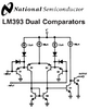
i was looking at datasheet of old opamp (lm393) and saw circuit scheme of opamp inside. Then i wonder it how things working inside. But i didnt clearly understand structure of opamp. Searched on internet and didnt found what i was looking for , or i couldnt searched correctly.
I m looking for text or a video to explaine how its works. For example on comparison operation , how its work. Which transistor getting switch and which is not etc.
Do you know any pages or videos to explain step by step ?
EDIT: ıt doesnt need to be lm393's inside. Every opamp will be good for me.
Last edited:

")
