Continue to Site

Welcome to our site!

Electro Tech is an online community (with over 170,000 members) who enjoy talking about and building electronic circuits, projects and gadgets. To participate you need to register. Registration is free. Click here to register now.

  • Welcome to our site! Electro Tech is an online community (with over 170,000 members) who enjoy talking about and building electronic circuits, projects and gadgets. To participate you need to register. Registration is free. Click here to register now.

Op-amp/transistor/transformer connection problem in inverter circuit

Status
Not open for further replies.
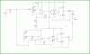
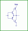
I have measured the current now in the circuit from post #38 with a scope across
a 1 Ohm resistor after the load resistor.
With no base resistor for the darlington pair i get a maximum current of 300mA
from the transistors to the load.
Since i need 3 times that to get to 1 amp, i will insert smaller transistors again
inbetween.
 
Concrete Question: Can i connect the small transistors Q1 and Q2 in that way to Q3,Q4 ?
Or is there more to connect like possible coupling caps or resistors?

**broken link removed**
 
Hi,

Looks like it should work.

There is one drawback to this output stage however. With the output transistors actually being two transistors as a Darlington Compound and the smaller driver transistors feeding their bases as voltage followers, the total voltage drop in the output is at least three diode drops. That means with a 12v supply and dual polarity output we have an effective +6v and -6v to work with, meaning that the maximum output voltage we can get from this output stage will be about 6-2.1=3.9v peak. That's about 2.76v RMS, which means the output power will only go as high as 0.762 watts. The RMS current will only reach about 0.276 amps.
To get a higher output current we'd have to increase the voltage that can get to the collectors of the two output transistors at least. Increasing the supply voltage to +26v will get us up to about 1 amp peak into a 10 ohm load.

Power consumption in the output transistors also has to be considered and heat sink chosen to match.
 
Mr.Al,
that is unfortunate.
I had the same thought yesterday while looking at it and looked out for a maybe
stronger high-current op-amp, that could maybe run the show alone or at least
allow to omit the small transistors. (TS925,LH0033)
It is however difficult to get a high-current one
with rail-to-rail capability and some would only be unity-voltage gain.
But good to know that the transistor connection is correct like this.

Another option would be to replace the sine source (XR2206) and do it
with something else that can deliver higher current already.
From initial reading about simple sine oscillators, i found that many are unstable
and have not so clean waves.
 
Last edited:
Hi again,


Well, the other amp you posted is a little better, having a current boosted voltage follower output stage. That's only got about 1 diode drop, which isnt bad really. That should work too without going to too much trouble.

You should be able to get this to work one way or another. You'll have to remember though that with a 12v power supply putting out a sine wave without using a bridge arrangement will mean only 6v peak is available even with a rail to rail device. That's only 0.6 amps peak into a 10 ohm load too.
With a bridge arrangement you can get 12v peak with a rail to rail, or about 10 or 11v peak with a standard transistor output. That's about 1 amp peak into a 10 ohm load.
For a bridge arrangement you build two such circuits and invert one of them with the op amp or another op amp. You then connect between the two outputs rather than between output and ground. That gives you twice the output voltage peak that you would get from a single output amplifier.
 
Thank you for that suggestion. The idea of doubling the circuit for a higher voltage swing is very good.
Just to make sure i understand it correctly, would it look like this?

**broken link removed**

This would also split the XR2206 4.8 mA output to 2 circuits for 2.4mA each right?
 
Last edited:
Hi,

Here is an example.

Note the gain of the top stage is 3 so the bottom stage gain should be the same, so the feedback resistor is different.
Also note R7 is the same as R1.
 

Attachments

  • Amplifier-02.gif
    Amplifier-02.gif
    12.4 KB · Views: 290
Last edited:
MrAl. Very kind of you to draw it. Thank you.
I will get the additional components and experiment with it and hopefully figure
out the right current flow between the transistors to reach the 1 Amp mark.
For the full voltage swing i would also probably have to change the feedback resistor ratio.
 
Hi again,

Unfortunately all those emitters (3 of them) in series means we'll lose a lot of voltage which will be significant at 12v. To get better you'll have to switch to a current boosted voltage follower output stage like your other amp link showed. Using only four transistors per amplifier, that allows up to about 9.5v peak output which would be 950ma peak into a 10 ohm load. This also requires a rail to rail output op amp.
 
Last edited:
...I had used 0.8mm wire for winding the primary, i will try a much smaller diameter wire which
will have more resistance....
You don't intentionally want more winding resistance since that reduces your efficiency. The no load current in a transformer is determined by the transformer inductance so you want the inductance to be high to give a low no-load current. Generally you use as large a wire size as will fit in the transformer winding space that will give you the inductance you need.

Edit: I agree with MrAl, you should use a circuit for the output stage such as you show in Post #40.
 
Last edited:
Hi,

I agree with Carl, although it does depend somewhat on the power output requirements and just how much more resistance you add. I think you meant to say that you would add more turns and thus end up with more resistance as a side effect in addition to the more turns. You may wish to clarify this.
 
Last edited:
I will need to change the circuit from post #40 to fit my circuit.
The resistors seem just to set the offset, the pot is probably for setting the output
loudness of that audio amplifier, so i think i can omit them.
Not sure about the diode and the cap though.
I read somewhere that connecting the darlington collectors together won't have such a strong
current amplification compared to the emitters chained, which is the main purpose of the
high hfe transistors here. Maybe i don't see the whole picture of the output stage as it works.
 
Last edited:
I will need to change the circuit from post #40 to fit my circuit.
It is an audio amplifier that is never used in an inverter circuit because its transistors are linear which makes them get very hot.
An inverter switches the transistors on and off so they do not waste power making heat. A low switching frequency produces a square-wave output that is not good to drive electronic products or a high switching frequency is used with pulse-width-modulation producing a sine-wave.
A class-D switching audio amplifier could be used in an inverter.

The resistors seem just to set the offset, the pot is probably for setting the output
loudness of that audio amplifier, so i think i can omit them.
Not sure about the diode and the cap though.
The resistors have symmetrical values so that the sine-wave output is also symmetrical.
The input pot is a volume control.
The diode and series resistor provide a small amount of bias current in the transistors to produce low distortion class-AB instead of the horrible crossover distortion of class-B.

I read somewhere that connecting the darlington collectors together won't have such a strong
current amplification compared to the emitters chained, which is the main purpose of the
high hfe transistors here. Maybe i don't see the whole picture of the output stage as it works.
The transistors are not connected as darlingtons. Instead they are connected as Sziklai pairs.
 
@Audioguru:
Thank you for the description.
What would you do instead of adapting the audio amp circuit?
Just keep the darlingtons in collector follower configuration?
If i would go full class-D switching i guess i would have to omit the existing circuit except for the XR2206 for the sine.
You gotta know that i don't need a very efficient circuit for this concerning the heat build-up.
I just wanted to do some experimental benchwork to educate myself on how to build simple inverters and i had set myself the 1 ampere mark (or more realistically 0.8 amps) for the amplifier to output to the primary to learn how to amplify correctly a relatively weak signal.
 
Last edited:
Since you need only 12V x 1A=12W then an audio amplifier circuit is fine.
Your circuit does not work because its max output is only about 7V p-p with a 12V supply and your transformer does not work at a frequency as low as 50hz.
 
Hi,

Here is a quick pic of the new output stage. This will help get up to the full voltage. Note the voltage drop caused by the first transistor is still around 0.7v, but the second transistor now can get near saturation which could mean only 0.3v drop. Since we only have an equivalent plus and minus 6 to work with relative to the average output voltage, that means we may get an equivalent plus and minus 5v out of each amplifier and when connected in a bridge arrangement that means plus and minus 10v across the load which into a 10 ohm load provides the 1 amp peak requirement.

As usual, the feedback resistor connects directly to the output which in this case is the two transistor collectors.

Something to watch out for is a little more distortion around the peaks when trying to drive this thing to the full amplitude possible Cutting back very slightly on the input amplitude should reduce that distortion if it is a problem.
 

Attachments

  • Ampl-03.gif
    Ampl-03.gif
    2.3 KB · Views: 237
Last edited:
@MrAl: I have built the circuit with the bridge-connected amplifiers.
Now i must start to determine possible resistor values for the bases of the first transistor stage. I believe i smoked them out by doing an initial test.
I should get a dozen of those hehe.
According to the datasheet, the op-amp puts out something like 40-50 mA, with the resistors used as per your schematic suggestion the voltage is exactly 5 Volt RMS.
With a hfe of 150 for the BC546/BC556, the collector current would be
750 mA.
The hfe of the TIP121/TIP126 is 1000.
Now, if i don't get that wrong only a base current of 1mA would be needed to get a collector
current of 1 amp at the 2nd transistor pair.
So is it the right approach to find a base resistor value for the first transistor stage that would give a collector current of 1mA? So 5kOhm resistor?
 
Last edited:
Maybe my calculation does not apply to a Sziklai pair configuration?

I have found a close schematic for such a configuration, but there were no values for the resistors
tp get an idea of their range :

**broken link removed**

The first stage is connected to VCC here too and in MrAl's diagram there is only the 2nd stage
connected to VCC.
 
Last edited:
After studying a lot of circuits, i realized that i am maybe too overcareful with the resistors and possibly this arrangement kind of regulates itself. So i went ahead and just connected the transistors with a 100 ohm base resistor and for one amplifier i got a current of 300mA RMS through the load resistor. This looks like a good figure.
 
Hi again,

Yeah the resistor cant be too critical because the gains of the transistors changes with temperature anyway. To work properly the circuit doesnt really need base resistors so all they would do anyway is provide for some simplified output current short circuit protection perhaps. You might try changing the values to see that you get full output yet limited current if you try to increase the load current too much.

The other circuit you posted has resistors going to Vcc to make sure the second transistor turns off completely when it's not supposed to be conducting.
 
Status
Not open for further replies.

Latest threads

Back
Top