Continue to Site

Welcome to our site!

Electro Tech is an online community (with over 170,000 members) who enjoy talking about and building electronic circuits, projects and gadgets. To participate you need to register. Registration is free. Click here to register now.

  • Welcome to our site! Electro Tech is an online community (with over 170,000 members) who enjoy talking about and building electronic circuits, projects and gadgets. To participate you need to register. Registration is free. Click here to register now.

LTspice simulation distortion function

Status
Not open for further replies.
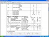
The beta for a transistor is listed on its datasheet. hFE is the DC current gain (beta) and hfe is the AC current gain (beta).
The beta is a range of numbers because each transistor and production run is different and changes with temperature change and with different currents.

Many inexpensive multimeters can measure the hFE at one low current.
 
is this beta.
 

Attachments

  • untitled.JPG
    untitled.JPG
    163 KB · Views: 392
The DC beta (hFE) is not 110.
The DC beta for a BC548 transistor at an ambient temperature of 25 degrees C and a collector current of 2mA is anywhere from 110 to 800.
The DC beta for a BC548A, BC548B or BC548C is selected in narrower ranges as shown further down the page.
The AC beta is not shown on the part of the datasheet you posted. It is a little less than the DC beta and is reduced as the frequency increases.
 
is this beta.

hi,
Has 'agu' has explained its a range of beta's for that transistor type, so there is a possible beta value from min to max. 110 thru 800.
 

Attachments

  • untitled.JPG
    untitled.JPG
    39.2 KB · Views: 333
Last edited:
So, for calculating i/p impedance of transistor for phase shift oscilator which beta value should be taken??
 
You should use a transistor that is selected for a low range of beta and with high beta. A BC548 has a beta from 110 to 800 which is too much range. Use a BC548C which has a beta of 420 to 800 then calculate the input impedance with its typical beta of 520. Then with a collector current of 3mA its input impedance is 4.5k ohms. The base bias resistors should have a current of 10 times the typical base current so their values will reduce the total input impedance to a little higher than the 2.9k ohms that you need. You can reduce the values of the base bias resistors so that the total input impedance is exactly 2.9k.

Your transistor has too much voltage gain so the output will be very badly clipped. Usually a limiting circuit is used to control the output amplitude to avoid clipping but your circuit is too simple and does not have it.
 
So, for calculating i/p impedance of transistor for phase shift oscilator which beta value should be taken??

hi,
You can modify the Beta value of a transistor in LTspice in the following way.
This will enable you to test the circuit with different Beta values.

Look for a file called standard.BJT in the following directory: C:\Program Files\LTC\LTspiceIV\lib\cmp\

If the transistor is in there, copy it and paste to another position in the list (say at the top) and then modify the "BF=" figure [beta] to your required value.
You can do this with each of your experimental values and then give each transistor a modified name.

For example, you could give a 2N3904 the name 2N3904_100 if you had given it a Beta of 100, save the file.

To use it, select the generic NPN transistor.
Place it on the schematic page.

Right click and choose "pick another transistor", select the modified transistor.

Be sure to make a back up copy of the standard.BJT before you edit it.
 
Last edited:
Look for a file called standard.BJT in the following directory: C:\Program Files\LTC\LTspiceIV\lib\cmp\

If the transistor is in there, copy it and paste to another position in the list (say at the top) and then modify the "BF=" figure [beta] to your required value.
You can do this with each of your experimental values and then give each transistor a modified name.

Hi, thanks i have done it, is very good method.

[LATEX]Be sure to make a back up copy of the standard.BJT before you edit it. [/LATEX]

what is this??
 
Hi, thanks i have done it, is very good method.

[LATEX]Be sure to make a back up copy of the standard.BJT before you edit it. [/LATEX]

what is this??

Its always a good idea to make a back up copy of any important file that you intend to modify, its possible you may corrupt the file data while experimenting.

If you do corrupt the 'file you are modifying' then replace it with the original backed up copy, so all is not lost....

EDIT:
How 520 is calculated??

Its NOT, its the typical value that you will use in the Zinp formula.
 
Last edited:
Hi, i found this ic in PCB SN74LVC244A OCTAL BUFFER/DRIVER WITH 3-STATE OUTPUTS. please tell why it is used in STB.
 
Hi, i found this ic in PCB SN74LVC244A OCTAL BUFFER/DRIVER WITH 3-STATE OUTPUTS. please tell why it is used in STB.

Do you mean the /OE [ output enable pin].?

If yes, then its used to set the output pins to ACTIVE or HiZ [high impedance] so that other Active/HiZ IC's outputs can be connected to the same logic lines.
 
I want to know i have STB (set of Box DTH), i opened it there was SMD IC called SN74LVC244A when i searched in goole the PDF shows it is OCTAL BUFFER/DRIVER WITH 3-STATE OUTPUTS, i thick buffer circuit means without loading input supply, output is given (High Z).

I want to know how to use this.
 
I want to know i have STB (set of Box DTH), i opened it there was SMD IC called SN74LVC244A when i searched in goole the PDF shows it is OCTAL BUFFER/DRIVER WITH 3-STATE OUTPUTS, i thick buffer circuit means without loading input supply, output is given (High Z).

I want to know how to use this.

As you know standard TTL IC's can only drive only a limited number of TTL inputs, the FAN out.

If you need to drive more inputs than the FAN out states for the IC, then a BUFFER/DRIVER IC can be used... check the FAN out figure on the datasheet.

Buffers are often used to drive long cable runs or 'capacitive' loads, by using a buffer IC which has a much higher drive capability than a standard IC, the signal quality is maintained.
ie: rising and falling edges of a logic signal and the signal voltage level.

https://en.wikipedia.org/wiki/Fan-out
 

Attachments

  • 000esp01.gif
    000esp01.gif
    61 KB · Views: 345
Last edited:
Hi, this is the images of IC and thus, fan mean motor one or something else??
 

Attachments

  • 14012011118.jpg
    14012011118.jpg
    179.6 KB · Views: 323
Here is my new ckt. pls check why the output waveform when connected to diode is irregular??

And pls give 7447 IC for LT Spice.

hi, after 15 days there is tech fest in my College and i want summit this project please see, should this will work???

This circuit is all about for, running led message with logic gates.
 

Attachments

  • ScreenHunter_01 Jan. 18 19.10.jpg
    ScreenHunter_01 Jan. 18 19.10.jpg
    116.4 KB · Views: 364
Last edited:
Why don't you use a decoder IC to drive the LEDs? Or use a counter/decoder IC?
Your circuit is not a schematic, it is just a hundred AND gates with Net names.
 
Status
Not open for further replies.

Latest threads

New Articles From Microcontroller Tips

Back
Top