Continue to Site

Welcome to our site!

Electro Tech is an online community (with over 170,000 members) who enjoy talking about and building electronic circuits, projects and gadgets. To participate you need to register. Registration is free. Click here to register now.

  • Welcome to our site! Electro Tech is an online community (with over 170,000 members) who enjoy talking about and building electronic circuits, projects and gadgets. To participate you need to register. Registration is free. Click here to register now.

LM358 Crossover Distortion Put To Rest (With Pics)

Status
Not open for further replies.

MrAl

Well-Known Member
Most Helpful Member
Hello there,


I had been mentioning a way to get rid of the LM358 crossover distortion for years and there's even an app note floating around on the web somewhere. We started talking about this again and some pic's posted showed some nasty crossover distortion so i decided to test it first hand.

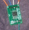
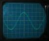
The board picture shows the board itself, minus the resistors used., while the scope picture shows the output waveform at 10kHz, amplitude 2v peak. Any slight distortion at the peak is caused by the frequency generator which uses a non linear technique which is not perfect, so the output wave looks just like the input wave. The gain is set up to be a voltage follower with output connected to the inverting input. The non inverting input has a 10k series resistor to protect the input stage if the power becomes disconnected for any reason, as the wave generator puts out it s own voltage signal.

As you can see from the scope pic, there is no noticeable crossover distortion. This happens with no load as well as any load going to the most negative supply, and i used a 1k resistor as the load for this test. The most negative supply is considered to be the ground reference, and the wave generator is set to have a suitable offset voltage so it can go plus and minus around that level on the input of the op amp.

The wave looks extremely clean near the zero crossing (and i zoomed in too at one point to check) and this is because the output has the resistor to ground.

Note the actual device used was an LM432 SMD package, but according to the old National data sheet it's the same amplifier as the LM358.
 

Attachments

  • LM432_Board.jpg
    LM432_Board.jpg
    164.5 KB · Views: 470
  • LM432_Test-1.jpg
    LM432_Test-1.jpg
    66.4 KB · Views: 406
Oh datasheet from texas instruments also said LM432 is similar to LM358, lol

Hi there,

Oh ok, that's good. Now that TI took over NS that isnt too much of a surprise :)

The LM432 has only one amp for general use unlike the LM358 because the other amp is tied up being used with the voltage reference, so it connects internally to the voltage reference. The op amp section i used was the 'free' one on pins 5, 6, and 7.
I will probably also test a regular SMD package LM358 too at some point but not sure when yet.
 
The LM358 dual and LM324 quad do not produce crossover distortion when they drive a resistor connected to ground like you did or to the positive supply because then one of the output transistors operates in class-A (and unfortunately gets hot).
Also since they are low power and do not have enough bias current for their class-B output transistors then the slew rate is so low that they have trouble with frequencies above 2kHz when the output level is high.

Your gain of only 1 resulted in lots of negative feedback and your frequency of 10kHz was maybe causing your opamp to attenuate crossover frequencies.
 
Hello again ag,

I believe your obsession with disliking the LM358 is founded in old information of some type that may have been spread by people that didnt know how to use the device. These devices are used in lots of commercial equipment which includes guitar amplifiers for example.

[1]
The LM358 dual and LM324 quad do not produce crossover distortion when they drive a resistor connected to ground like you did or to the positive supply because then one of the output transistors operates in class-A (and unfortunately gets hot).
Yes that is correct. But once biased properly the results are easy to see on the scope picture of the actual device and it shows a clean waveform.

[2]
Also since they are low power and do not have enough bias current for their class-B output transistors then the slew rate is so low that they have trouble with frequencies above 2kHz when the output level is high.
They work fine within the specs they were designed for just like any other op amp would work with the same specs. Not all op amps are designed to put out 50 megaamperes at 2 gigahertz with a slew rate of 50 megavolts per microsecond. Any op amp with a GBW of 1MHz and slew rate of 0.5v/us will act the same way. If you want faster then you look for faster, but if you dont need faster than you can use ANY op amp with these specs, and ANY includes this one.

[3]
Your gain of only 1 resulted in lots of negative feedback and your frequency of 10kHz was maybe causing your opamp to attenuate crossover frequencies.
In #1 above you said the crossover was eliminated with the proper output biasing, so no need to rethink this aspect of it. It doesnt really matter that the gain was 1 i used that because it was easier to set up the test and besides using this for a buffer is a common use anyway. But the 10kHz attenuation idea is just not correct because the 2v peak wave looks the same at 100Hz, 1kHz, and 10kHz, and those three frequencies were used for the tests. Of course the slew rate limits going too high, but that's the same for any op amp with a slew rate of 0.5v/us.

[4]
Price. The cost for one device is less than a dollar USD. In fact, you can get almost 3 for a dollar at just 38 cents each and in quantities of 2500 you can get them for just 8 cents each. Yes, that's 12 for a dollar :)

[5]
I could post applications for this device, but they are so numerous it would take up quite a bit of space. Projects ranging from amplifiers to battery chargers to frequency converters to full range bulb dimmers...just to name a few.
 
Last edited:
As per AG's observations, MrAl could you test the amp with a plus and minus supply with the load to common (midpoint of the supplies) or connected to the midpoint of two 2kΩ resistors in series connected from the V+ to ground, since that will increase the chance of observing crossover distortion?
I can see how using a single supply with a single resistor to ground minimizes that type of distortion.
 
I know the LM358. The LM358 is a friend of mine. I started designing with it the year it came out. But I'm with ag on this one. It is the greatest 2-wire intercom part in the world because it can survive almost anything up to a direct lightning strike, and a mile of cable across a golf course picks up a lot of stuff. But a guitar amp is almost as limited a set of requirements as a voltage follower bench test. For real audio, like a phono preamp or an active filter, it falls apart very quickly because of its limited GBW. The output stage bias trick cannot compensate for its inherent internal non-linearities caused by its low-gain PNPs, or its high input noise caused by its low input stage design current. Hell of a part, but an audio part only in a very restricted sense.

ak
 
Maybe the MC358 was used in geetar amplifiers because they want all the distortion as they can get. It was designed for low power so the bias current on the output transistors was so low that they produce crossover distortion since they operate in class-B instead of class-AB. I think it is wrong to force an output transistor to use a very high current continuously in class-A.

I use MC33172 dual low power opamps for portable low power supply voltage and current audio applications since they have the same input common-mode voltage range all the way down to 0V, lower power supply current and the same low power supply voltage as the LM358 but they have no crossover distortion and work well up to 35kHz.
 
As per AG's observations, MrAl could you test the amp with a plus and minus supply with the load to common (midpoint of the supplies) or connected to the midpoint of two 2kΩ resistors in series connected from the V+ to ground, since that will increase the chance of observing crossover distortion?
I can see how using a single supply with a single resistor to ground minimizes that type of distortion.

Hello there Carl,

Well, we already know that connecting ONLY a load to the output to a central ground (dual supplies) will allow crossover distortion. We know that because it's been tested and scope picture posted in another thread clearly shows crossover distortion.

BUT, the solution is to connect A SECOND resistor from the output to the MOST NEGATIVE supply. The load can go anywhere it needs to go, form output to negative, from output to ground. But without that SECOND resistor there will be crossover distortion. The SECOND resistor is what forces the op amp to work in a more linear class which prevents ANY crossover distortion because then there is no crossover, even when the actual load goes from output to central ground.

So you see the device CAN product crossover distortion, but with an extra resistor on the output (of the right value of course) there is NO crossover distortion anymore because there is no crossover.
 
I know the LM358. The LM358 is a friend of mine. I started designing with it the year it came out. But I'm with ag on this one. It is the greatest 2-wire intercom part in the world because it can survive almost anything up to a direct lightning strike, and a mile of cable across a golf course picks up a lot of stuff. But a guitar amp is almost as limited a set of requirements as a voltage follower bench test. For real audio, like a phono preamp or an active filter, it falls apart very quickly because of its limited GBW. The output stage bias trick cannot compensate for its inherent internal non-linearities caused by its low-gain PNPs, or its high input noise caused by its low input stage design current. Hell of a part, but an audio part only in a very restricted sense.

ak

Hi,

Yes, there are limitations just as there are with any op amp. But singling this one out as a 'problem' device is not logical when any op amp with the same ratings will do nearly the same thing, which in this case, is limit the useable output frequency with amplitude.
So putting it another way, we dont drive a golf cart and expect it to act like a BMW, but then again we dont drive a BMW on the golf course either.
 
Maybe the MC358 was used in geetar amplifiers because they want all the distortion as they can get. It was designed for low power so the bias current on the output transistors was so low that they produce crossover distortion since they operate in class-B instead of class-AB. I think it is wrong to force an output transistor to use a very high current continuously in class-A.

I use MC33172 dual low power opamps for portable low power supply voltage and current audio applications since they have the same input common-mode voltage range all the way down to 0V, lower power supply current and the same low power supply voltage as the LM358 but they have no crossover distortion and work well up to 35kHz.


Hello again,

The output transistor is not forced to operate with "very high current". The output resistor is selected as needed. For example, for a light load a higher value resistor can be used. For my test, the output resistor draw a "very high current" of a whole 2ma peak.

Again, the crossover is only observed in certain applications where there is no extra output resistor. The extra resistor prevents the crossover.

The MC33172 is a HIGHER QUALITY op amp so it ACTS like a HIGHER QUALITY op amp. What else would you expect? It's also higher priced. I can easily list 10 other op amps that are better than the LM358 but i can also list 10 other cars that are better than a Yugo, but that does not mean we can not drive a Yugo to the store and back (to purchase 10 LM358 chips :) ).
 
Hello again,

I have the actual LM358 ready now so i will be testing soon. Of course the results wont be too much different, but i needed another excuse to practice SMD soldering. Back when i worked in the industry, we never needed SMD packages but today many chips only come in SMD os you have to be able to do it if you want to try out those chips. I also bought some solder paste and it was expensive enough that i wont let it sit around forever without using it :)

I checked the specs on the MC33172 chip and they look pretty impressive. I might actually get a few to test soon. Prices isnt too bad, about 75 cents each and about 34 cents each in quantities of 2500. The price is somewhat comparable to the LM358 if you figure in the specs. That is, the price is 4 times higher but the specs are all 4 times higher too (GBW and SlewRate). I may be able to use one of these chips in my special power supply as the chip i was going to get is about 6 dollars. It has much higher specs but i may be able to get around that. The LM358 though i feel is too slow for higher quality power supply error amps. Useable yes, but i like faster response.
 
The MC3317x has a very low maximum output high current.
The MC3407x has even better spec's than the MC3317x but draws more power supply current. It is not made in a though hole package anymore so a TLE214x can be used to replace it.

In my career, money grew on trees so the cost of parts did not matter.
 
Hello again,

I'll check out that chip too next.

Funny you should mention another part that is not made in DIP package anymore. Yesterday i had to identify pin 1 on a SMD package (LM358) and the old data sheet i had did not show where pin 1 was on the SO8 package although it did show for the DIP package and two other package types. After downloading a more current data sheet from the manufacturer (which was ST), i found that they had a note "removed DIP package" on the data sheet, and NO MORE DIP package being shown!
Maybe DIP packages are going the way of the vacuum tube :)
 
I also bought some solder paste and it was expensive enough that i wont let it sit around forever without using it :)

Solder pastes, don't they have expiration date?
 
Hello there,

Well, they are supposed to yes, but for example mine has no date on it at all.

I have read of over 2 years life, but i also read about two failure modes one of which is correctable.

The first is the interaction of the rosin and the solder particles. The solder particles have an oxide on the outer surface that protects them from sticking together. As the rosin works on the oxide layer it degrades and so the solder particles can start to stick together forming large clusters instead of tiny balls. This would cause a problem in spreading the paste over the ic chip pins. If it got too bad, it would have to be thrown out i think.

The second is the amount of rosin or condition of the rosin. The paste dries out and supposedly the cause is because the rosin dries out. By adding some extra flux and stirring it into the paste, it becomes wetter again and starts to work like new.

I dont have much experience with this stuff yet though so i dont know how long the above flux addition owrks. If it gets too old it may not work anymore, i dont know yet.

But interestingly, solder companies also date their wire solder. I think Kester dates theirs between 2 and 3 years, but anybody who has a roll of solder at home knows that it still works after many years. I have a roll from the late 1970's that still works great so you'd never know it was that old (rather thick wire like AWG gauge 16 or something like that with rosin core).
The internal flux properties might change over time making it a little harder to use eventually.

The wire solder might be dated for commercial use. Way back when i worked for Singer Kearfott i worked in one of the computer departments, and someone from engineering gave me a roll of solder that was almost full. If i remember right he said it was because it was too old for their use as they rotate their stock and get rid of the older stuff. It still worked pretty well for me. It was thin rosin core solder 60/40 metal content.
 
Many ICs are made today in a "bumps on bottom" case that needs to be soldered in an oven I guess.
 
.............
Maybe DIP packages are going the way of the vacuum tube :)
I'm afraid so. Except for repair and building of legacy devices, and hobbyists, no one uses DIP packages anymore, so the volume is too small for manufacturers to economically keep building devices in that package style. :(
Because of large inventories many old devices will still be around for years in DIP packages, but no new devices will be.
 
Many ICs are made today in a "bumps on bottom" case that needs to be soldered in an oven I guess.

Hi again,

Yes, but lucky i did not need that kind of package yet :)
I would probably have to have a board that was made for that package too unless it only had a few pins or something.
The boards i use for the SMD packages now are those "surf" boards that convert SMD to a sort of DIP package so i can hook wires up to it for testing.
 
I'm afraid so. Except for repair and building of legacy devices, and hobbyists, no one uses DIP packages anymore, so the volume is too small for manufacturers to economically keep building devices in that package style. :(
Because of large inventories many old devices will still be around for years in DIP packages, but no new devices will be.

Hi,

Yeah, that is unfortunate for the hobby unless you are willing to do at least some SMD soldering.
I did a TSSOP-28 pin package once, but it's really a pain and at the time i had no solder paste so had to use regular solder. I had to make a special tip for the iron that was very narrow. Later i discovered another way to do it using a big blob of solder that covers the entire row of pins even between pins and then use solder wick to pick up the unwanted solder. Have not actually tried that idea yet though.

The solder paste is some amazing stuff though. You can smear it across ALL pins even in between pins, and when you hit it with the hot air tool the solder melts and finds it's way to the pins and pads and only the pins and pads and anything between pins gets sucked onto the adjacent pin or pad through what seems to be very strong surface tension and cohesion of the solder. I would think the cohesion of the melted solder paste is stronger than the adhesion to the non metalized part of the PC board so all the solder finds it's way to the metal parts only. It's pretty amazing to watch it crawl to the pins. I should have taken a video, but i know there are some on the web already. It's not magic either, it really works.
 
Status
Not open for further replies.

Latest threads

Back
Top