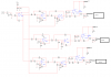
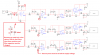
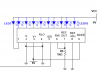
Your filters are Sallen Key highpass and lowpass but the filters in the article are Multiple Feedback bandpass filters which are completely different.
Why do you have an opamp at the input with very high gain of 21.3? It drives a volume control that messes up the filter fed from it. Also, the input opamp with very high gain will easily be overloaded. The volume control should be at its input, then it directly drives all 3 filters without coupling capacitors. Then it biases the lowpass filter opamps.
Why does the original circuit use an opamp for its "virtual ground" when it bias the other opamps with a very low current? The voltage divider that feeds the virtual ground opamp can bias hundreds of opamps.
The input opamp in the original article is not an audio amplifier, it is a modern opamp that can drive a load as low as 600 ohms that is not in the original circuit. Your opamp from an LM324 is fine to drive 5hree 20k volume controls.
I corrected your tiny schematic that is covered with Multisim chicken pox dots.
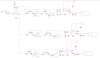