I posted about "lock" footprints in the thread the other day, but this is too important to be buried in a thread if you design your own circuit boards.
When soldering male header pins to a printed circuit board, it can be difficult to get the connector perpendicular to the board. All too often, when you look at the header after soldering, it's at an angle. Trying to square it up results in burned fingers and cuss words, but little change in the final result.
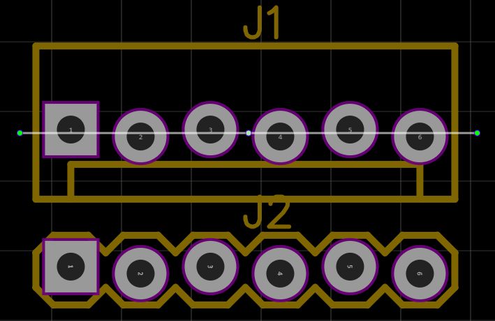
A clever guy named Pete Lewis at Sparkfun came up with a simple way to solve this problem. Alternating pads for a header connector are placed just a bit above the connector centerline and below the centerline., providing a slight interference fit (depending on hole plating) and keeping the connector perpendicular to the board when you insert it. Getting perfect connector alignment is simple with this small change in the PCB footprint. The illustration below shows the small offset from the connector centerline. The horizontal white line is the connector centerline.

The (sometimes) interference fit has a great side effect. Using this footprint for ICSP programming allows you to "plug in" a header connector if you'll only be programming the board a few time.
If you use EasyEDA, please feel free to use my library of lock connector footprints. For headers and Molex KK connectors, I've created patterns for 3 pins up to many. You should be able to find them under owner "jonchandler". I have modified my footprints from those supplied by Sparkfun - Sparkfun footprint origin at pin 1; I put the origin at the center of the pad group (as God intended). When you rotate my footprints, they stay centered in the same place on the board.
Sneaky Footprints - SparkFun Electronics
When soldering male header pins to a printed circuit board, it can be difficult to get the connector perpendicular to the board. All too often, when you look at the header after soldering, it's at an angle. Trying to square it up results in burned fingers and cuss words, but little change in the final result.
A clever guy named Pete Lewis at Sparkfun came up with a simple way to solve this problem. Alternating pads for a header connector are placed just a bit above the connector centerline and below the centerline., providing a slight interference fit (depending on hole plating) and keeping the connector perpendicular to the board when you insert it. Getting perfect connector alignment is simple with this small change in the PCB footprint. The illustration below shows the small offset from the connector centerline. The horizontal white line is the connector centerline.
The (sometimes) interference fit has a great side effect. Using this footprint for ICSP programming allows you to "plug in" a header connector if you'll only be programming the board a few time.
If you use EasyEDA, please feel free to use my library of lock connector footprints. For headers and Molex KK connectors, I've created patterns for 3 pins up to many. You should be able to find them under owner "jonchandler". I have modified my footprints from those supplied by Sparkfun - Sparkfun footprint origin at pin 1; I put the origin at the center of the pad group (as God intended). When you rotate my footprints, they stay centered in the same place on the board.
Sneaky Footprints - SparkFun Electronics


