I always hate it when I lay out a printed circuit board and discover I haven't left enough clearance around mounting holes to tighten up a nut or spacer with a nut driver, or to even get a spacer in place. This is a simple method to eliminate that problem.
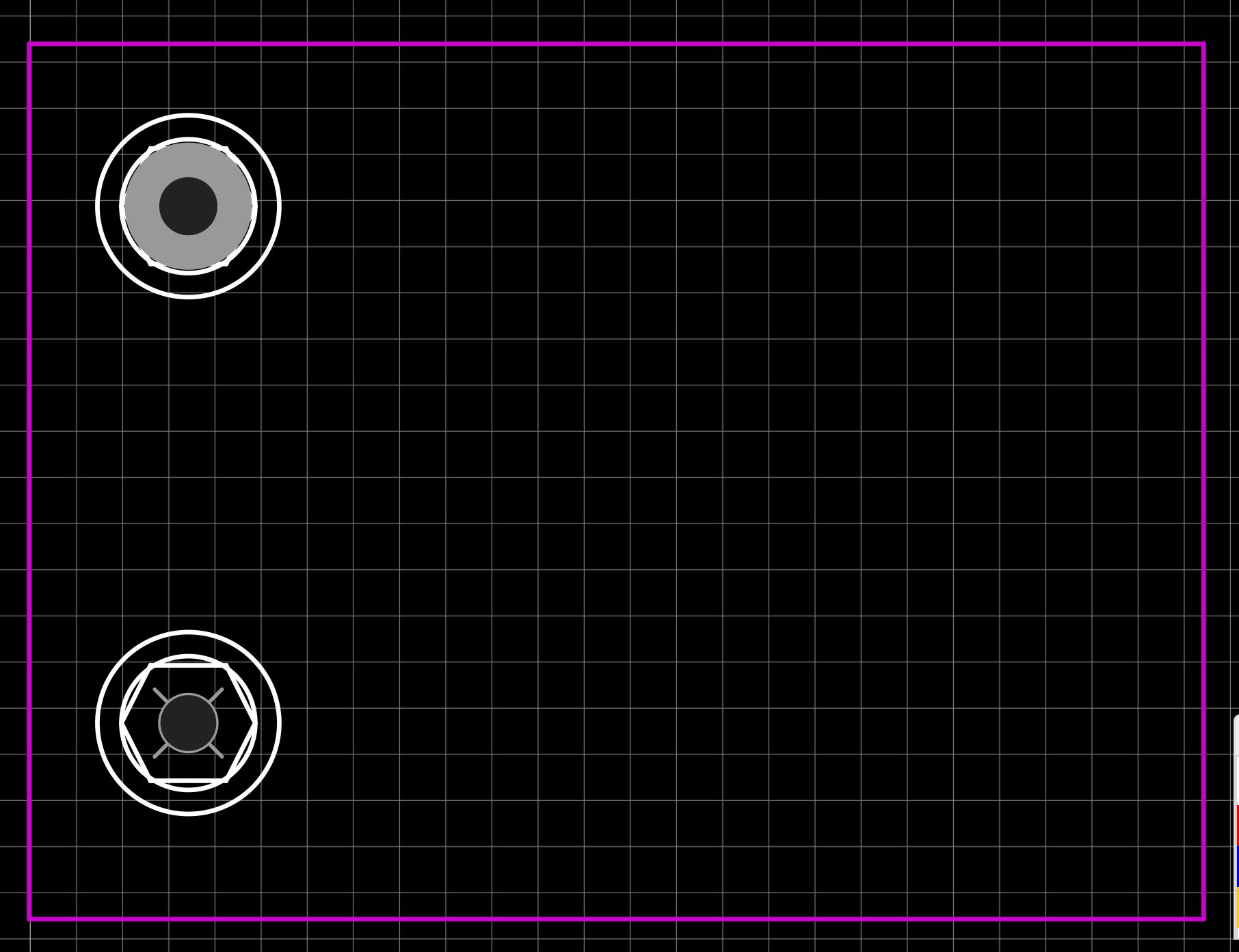
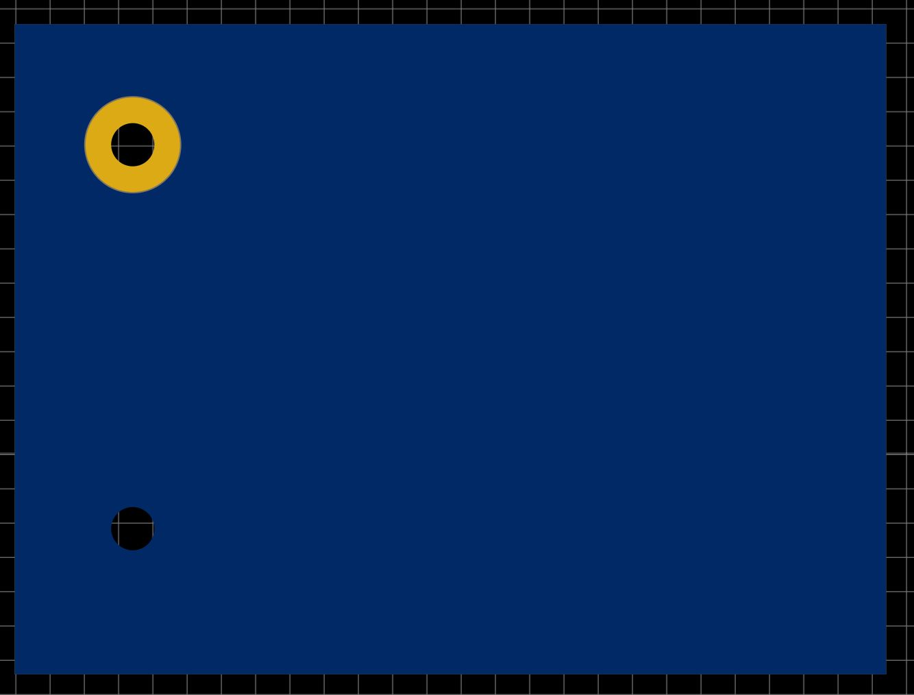
I designed a mounting hole "component" for 3mm or 4-40 screws that include the clearance for a nut and nut driver in the PCB document layer. These lines, which won't show up on the finished circuit board, show the clearance needed for a nut (where you always want to avoid placing components) and a nut-driver (where it is desirable to avoid placing components. I have two different mounting hole components, one with a pad, and the other with just a hole.

The white lines are in the document layer, so they don't show up on the circuit board.

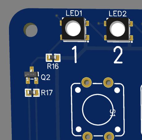
Here's an actual board layout, showing the results of using these mounting hole components.

I try to keep traces out of the nut driver clearance area, to avoid any possible damage if a nut driver has a sharp edge.
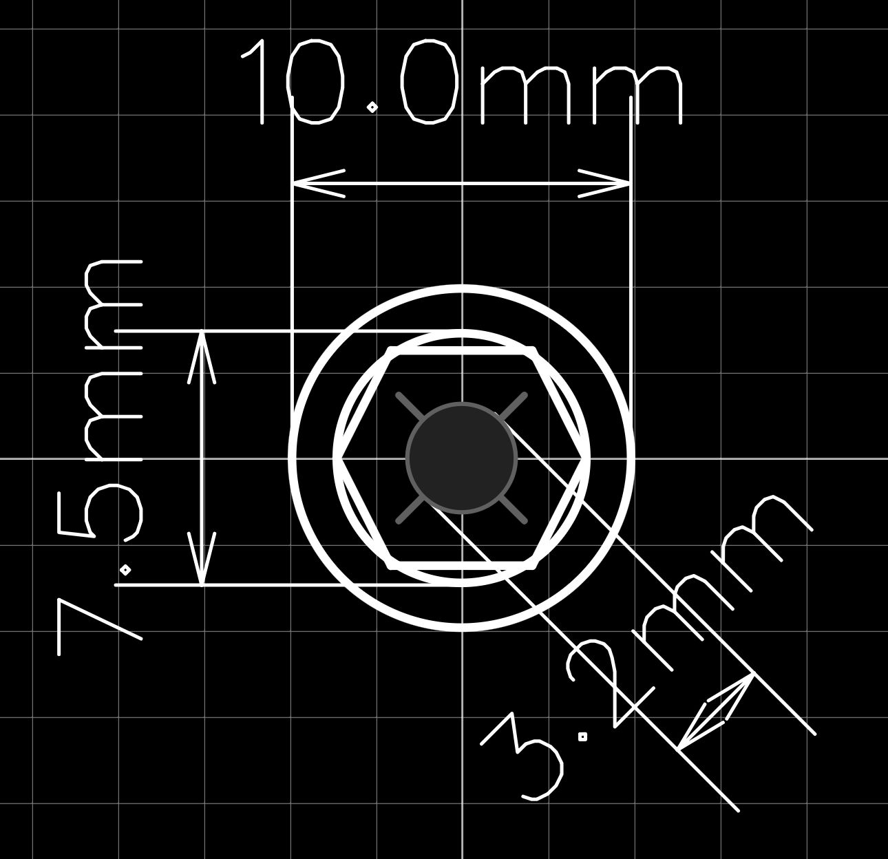
Here are the dimensions I used for 3mm / 4-40 mounting hardware. The are close enough to the same size that the same diameter hole and pattern work for both. A few minutes laying out a footprint like this saves a lot of time during board layout and poor board designs.


I designed a mounting hole "component" for 3mm or 4-40 screws that include the clearance for a nut and nut driver in the PCB document layer. These lines, which won't show up on the finished circuit board, show the clearance needed for a nut (where you always want to avoid placing components) and a nut-driver (where it is desirable to avoid placing components. I have two different mounting hole components, one with a pad, and the other with just a hole.
The white lines are in the document layer, so they don't show up on the circuit board.
Here's an actual board layout, showing the results of using these mounting hole components.
I try to keep traces out of the nut driver clearance area, to avoid any possible damage if a nut driver has a sharp edge.
Here are the dimensions I used for 3mm / 4-40 mounting hardware. The are close enough to the same size that the same diameter hole and pattern work for both. A few minutes laying out a footprint like this saves a lot of time during board layout and poor board designs.
